SSZT859 December 2017 LPV811 , LPV821 , TLV8541
Heightened accuracy and speed in an operational amplifier (op amp) has a direct relationship with the magnitude of its power consumption. Decreasing the current consumption decreases the gain bandwidth; conversely, decreasing the offset voltage increases the current consumption.
Many such interactions between op amp electrical characteristics influence one another. With the increasing need for low power consumption in applications like wireless sensing nodes, the Internet of Things (IoT) and building automation, understanding these trade-offs has become vital to ensure optimal end-equipment performance with the lowest possible power consumption. In the first installment of this two-part blog post series, I’ll describe some of the power-to-performance trade-offs of DC gain in precision nanopower op amps.
DC Gain
 Figure 1 Inverting Op Amp
 Figure 2 Noninverting Op Amp
These configurations resulted in inverting and noninverting op amp closed-loop gain equations, Equations 1 and 2, respectively:
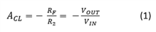
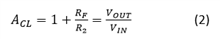
where ACL is the closed-loop gain, RF is the value of the feedback resistor and R2 is the value of the resistor from the negative input terminal to signal (inverting) or ground (noninverting).
These equations are a reminder that DC gain is based on resistor ratio, not resistor value. Additionally, the “power” law and Ohm’s law show the relationships between resistor value and power dissipation (Equation 3):
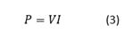
where P is the power consumed by the resistor, V is the voltage drop across the resistor and I is the current through the resistor.
For nanopower gain and voltage divider configurations, Equation 3 tells you that, in order to minimize power dissipation, you need to minimize the current consumption by the resistor. Equation 4 helps you understand the mechanism to do that:
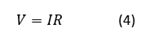
where R is the resistor value.
Using these equations, you can see that you must choose large resistor values that provide both the gain you need while minimizing power dissipation (and therefore power consumption). If you don’t minimize current through the feedback path, you’ll lose the benefit of using nanopower op amps.
Once you’ve determined what resistor values will meet your gain and power-consumption needs, you’ll need to consider some of the other op amp electrical characteristics that will affect the accuracy of signal conditioning. Summing several small systemic errors inherent in nonideal op amps will give you the total offset voltage. The electrical characteristic, VOS, is defined as a finite offset-voltage number between the op amp inputs, and describes these errors at a defined bias point. Please note that it does not describe these errors across all operating conditions. To do that, you must consider the gain error, bias current, voltage noise, common-mode rejection ratio (CMRR), power-supply rejection ratio (PSRR) and drift. Covering all of these parameters is beyond the scope of this post, but let’s look at VOS and drift – and their influence in nanopower applications – in a bit more detail.
Real-world op amps exhibit VOS across their input terminals, which can sometimes be a problem in low-frequency (close to DC) precision signal-conditioning applications. In voltage gain configurations, the offset voltage will gain up along with the signal being conditioned, introducing measurement errors. In addition, the magnitude of VOS can change over both time and temperature (drift). Therefore, in low-frequency applications requiring fairly high-resolution measurements, it’s important to select a precise (VOS ≤ 1mV) op amp with the lowest possible drift.
Equation 5 calculates the worst-case VOS over temperature:

Now that I’ve covered theory, including choosing large resistor values to create gain ratios and op amp accuracy for low-frequency applications, I’ll go over a practical example using two-lead electrochemical cells. For two-lead electrochemical cells which often emit very small signals of low frequency, and are used in diverse portable sensing applications like gas detection and blood glucose monitoring, choose a low-frequency (<10kHz) nanopower op amp.
Using oxygen sensing (see Figure 3) as the specific application example, assume that the maximum concentration of the sensor outputs 10mV (converted from current to voltage by a manufacturer-specified load resistor, RL) and the full-scale output of the op amp is 1V. Using Equation 2, you can see that ACL needs to be 100, or RF needs to be 100 times larger than R2. Choosing values of 100MΩ and 1MΩ, respectively, gives you a gain of 101, and these resistor values are large enough to limit current and minimize power consumption.
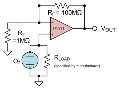
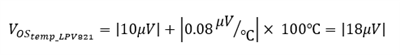
To minimize offset error, the LPV821 zero-drift nanopower op amp is a good choice. Using Equation 5 and assuming an operating temperature range from 0°C to 100°C, the worst-case offset error introduced by this device will be:
Another good choice is the LPV811 precision nanopower op amp. Using its data sheet to gather the necessary values plugged into Equation 5 gives you:
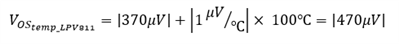
(Note that the LPV811 data sheet does not specify a maximum offset voltage drift limit, so I am using the typical value here.)
If you were to use a general-purpose nanopower op amp like the TLV8541 instead, those values would result in:
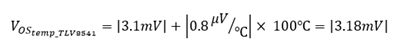
(The TLV8541 data sheet also does not specify a maximum offset voltage drift limit, so I again used the typical value here.)
As you can see, the LPV821 op amp is the best choice for this application. With 650nA of current consumption, the LPV821 can sense changes in the output of the oxygen sensor down to 18µV or lower, and introduces a maximum offset gain error of only 2.3mV. When you need both extreme precision and nanopower consumption, a zero-drift nanopower op amp will provide the best possible performance.
Thanks for reading this first installment of the “How to make precision measurements on a nanopower budget” series. In the next installment, I’ll discuss how ultra-precise nanopower op amps can help in current-sensing applications. If you have any questions about precision measurements, log in and leave a comment, or visit the TI E2E™ Community Precision Amplifiers forum.
Additional Resources
- Download the LPV821, LPV811 and TLV8541 data sheets.
- Read about designing on a nanopower budget in these TI TechNotes:
- Check out all of TI’s amplifier devices.