SSZT924 october 2017 DS90UB933-Q1 , DS90UB934-Q1 , DS90UB935-Q1 , DS90UB936-Q1 , DS90UB953-Q1 , DS90UB953A-Q1 , DS90UB954-Q1 , DS90UB960-Q1
As advanced driver-assistance system (ADAS) applications such as front camera and camera-monitoring systems (CMS) use camera imagers above a 2MP resolution more widely, video data-transfer speed requirements increase. These ADAS architecture shifts are driving the next generation of Flat Panel Display (FPD)-Link™ III devices. FPD-Link III serializer/deserializer (SerDes) devices are moving from existing parallel interface product families such as TI’s DS90UB933-Q1 and DS90UB934-Q1 to the newer Mobile Industry Processor Interface (MIPI)-compliant 4Gbps DS90UB953-Q1, DS90UB935-Q1, DS90UB951-Q1 and DS90UB953A serializers, and DS90UB954-Q1, DS90UB958-Q1 and DS90UB936-Q1 deserializers.
The DS90UB95x SerDes family includes new features that enable much more streamlined camera designs. The first major enhancement to moving from digital video port (DVP) format on imagers and accompanying serializer devices is the MIPI Camera Serial Interface (CSI)-2 video interface. This interface enables data-transfer rates as high as 832Mbps on each of the four CSI-2 differential lanes. With these faster rates, 2MP at 60fps video and above is possible. The 100MHz pixel-clock frequency limits the parallel interface format; since this parallel format has predetermined data bits, it is usually capped at a 10- or 12-bit resolution.
The CSI-2 format uses four differential lanes for data and one differential lane for the clock, which requires routing five length- and impedance-matched differential pair traces between the imager and serializer but uses only 10 pins. For the parallel interface, in addition to the 10 or 12 pins required for each of the video data bits, this format also requires vertical sync (VSYNC), horizontal sync (HSYNC) and a pixel clock (PCLK). So now, a 1MP imager at 60fps uses 12 bits for data and three video synchronization signals for a total of 15 pins. As I mentioned, CSI-2 drastically simplifies designs for camera modules. Also, with this interface’s flexibility, you can use radar modules because the interface format is compatible with those devices.
Interface format and speed between imager and serializer is only one aspect of the new DS90UB95x. These devices preserve the back-channel I2C communication capability from deserializer to serializer to enable remote-module initialization from a host processor. While this feature is standard on FPD-Link III devices, the DS90UB95x family improves the ability to use the back channel at speeds up to 100Mbps versus the previous 2.5Mbps on DS90UB93x devices. The speed increase on the back channel also enables faster imager setup times, which is becoming especially important as vehicles begin including autonomous capabilities. If the vehicle can't take over as soon as possible after starting, there could be a gap in time when the driver believes the car is taking action while it is not.
Another important feature included in DS90UB95x devices is the capability for synchronous clocking. The DS90UB953-Q1, DS90UB935-Q1, DS90UB951-Q1 and DS90UB953A-Q1 Serializers are now able to get an input reference clock over the back channel from the DS90UB954-Q1 Deserializer or DS90UB960-Q1 Deserializer Hub for example. This capability is a great benefit because the system design can become simpler, smaller and less expensive on the camera module side. Previous camera modules required an on-board reference clock oscillator to supply the necessary input frequency for the serializer so that the serializer could then supply a specific clock frequency to the imager for PCLK. While this was sufficient, it did result in a drawback. If different applications around the vehicle were going to use the imager, or 10 bits instead of 12 bits were used in certain situations, achieving a specific PCLK frequency required a different oscillator.
For example, let us say a 1MP imager in 12-bit mode required 60fps; that would require a 66.66MHz oscillator because PCLK is derived from REFCLK to be 1.5 times its frequency. You would not be able to use this same oscillator in 10-bit mode, however, because in that mode, PCLK is two times the REFCLK and would be above the 100MHz PCLK limit for the DS90UB933-Q1.
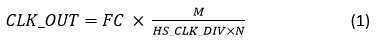
The synchronous clock capability enables the supply of a register-tunable CLK in the DS90UB953-Q1 to the imager based on the REFCLK supplied from the DS90UB954-Q1 over the back channel. Figure 1 shows REFCLK, the back channel synchronous clock used to generate CLK_OUT. You do not need CLK_IN in synchronous mode, which allows for much more flexibility when using the imager in different operation modes.
 Figure 1 Synchronization Clocking
Setup
Figure 1 Synchronization Clocking
SetupIn order to change CLK_OUT, the DS90UB953-Q1 has CLKOUT CTRL 0 and CLKOUT CTRL 1 at registers 0x06 and 0x07. These two registers contain the values available for M, HS_CLK_DIV and N. FC is the forward-channel data rate of the FPD-link III channel. As an example, if the REFCLK for the DS90UB954-Q1 shown in Figure 1 was 25MHz but the CLK_OUT supplied to the imager needs to be 24MHz, the values HS_CLK_DIV=2, M=3 and N=0xFA would ensure an FC rate of 4Gbps. Take care to convert N=0xFA to decimal format when calculating in order to ensure the correct clock frequency for CLK_OUT; see Equation 1.
As we know, scalability within the ADAS sector is going to be imperative. As imagers become more advanced, our interface and communication techniques must keep up. The new high-speed DS90UB953-Q1 and DS90UB954-Q1 combine simplicity and advanced technology to enable many varieties of driver-assistance applications, while paving the way to a more autonomous vehicle.
Additional resources:
- Learn more about TI’s ADAS reference designs
- Learn more about the Automotive 2-MP Camera Module Reference Design with MIPI CSI-2 Video Interface, FPD-Link III and POC
- Read this blog post:
- Read this application note:
- Learn more about FPD-Link III in the Learning Center