SSZT935 october 2017 CSD95490Q5MC , TPS53667
While a proper high-current power-stage layout is always important in DC/DC applications, paying attention to regulator signal routing during printed circuit board (PCB) layout is more important than ever. Revision 1.3 of the popular PMBus protocol brings with it faster 1MHz clock speeds as well as the option of a high-speed 50MHz AVSBus. These digital lines, along with the quick edged pulse-width modulation (PWM) signals associated with each regulator phase must be properly routed to avoid hampering the ever-increasing analog performance requirements of today’s applications. With the addition of smart power stages into the mix, you also have to factor more analog sense lines into your PCB layout in order to report output current and FET temperature back to the controller. Keeping it all straight can be an engineer’s nightmare.
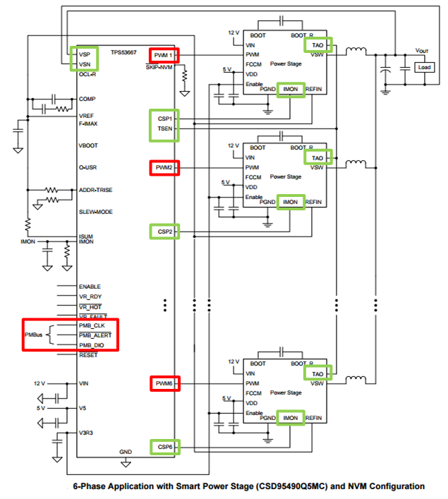
Figure 1 shows a six-phase buck regulator using the TPS53667 controller and CSD95490Q5MC smart power stage, with the fast edge signals highlighted in red and sensitive analog runs in green. In an ideal scenario, PWM1 to PWM6 and the PMBus lines would be placed on a separate layer from the current, voltage, and temperature sense traces with a shielding ground plane in-between. In space-constrained applications however, such separation is not always possible and one thing you have to watch out for in that case is crosstalk.
 Figure 1 Multiphase Buck Regulator
Using the TPS53667 and Smart Power Stages
Figure 1 Multiphase Buck Regulator
Using the TPS53667 and Smart Power StagesWhen routing two traces in parallel, some amount of coupling – capacitive, inductive or both – occurs between the two. In digital systems, there should be sufficient noise margin to prevent any sort of corruption, but when a noisy PWM signal is routed next to an analog current-sense trace, as shown in Figure 2, the accuracy of the current-monitoring system is affected.
In the best-case scenario, the controller reports an incorrect current reading to the system. In the worst case, the crosstalk is bad enough to trigger a false overcurrent event and shut the system down. If the VOUT sense lines are routed incorrectly instead, regulation accuracy and loop stability may be negatively affected.
 Figure 2 Incorrect Routing
Example
Figure 2 Incorrect Routing
ExampleCrosstalk is influenced by a number of parameters, including the spacing between traces, the height above or below a shielding plane, signal rise times, and the length at which the signals are routed in parallel together. For the TPS53667, the controller design sets the PWM edge time while the PMBus specifications set the rise times for the communication lines. Since this is a space-constrained application, we’re assuming we cannot move the PWM and current sense pin (CSP) traces to separate layers. This leaves the spacing of the traces and the thickness of FR4 as the only handles available to minimize crosstalk. See Figure 3.
 Figure 3 Microstrip (Left) and
Stripline (Right) Layout Examples
Figure 3 Microstrip (Left) and
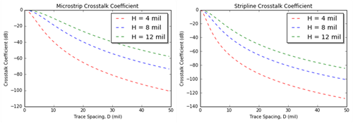
Stripline (Right) Layout ExamplesAs trace spacing and height are varied, you can draw several key conclusions from Figure 4 in order to combat crosstalk and provide an optimal layout. The goal is to maximize spacing between traces as much as possible, while at the same time making the layer thickness as thin as fab house constraints will allow. Confining the traces to internal layers to create a stripline also cuts down on coupling between traces. Finally, for the best performance and added insurance against unwanted crosstalk, place a ground trace or ground fill between high-speed signals and sense lines for as long as they are in parallel with one another, as shown in Figure 5.
 Figure 4 Crosstalk Coefficients in
Decibels for Microstrip (Left) and Stripline (Right) Layouts
 Figure 5 Optimized Layout
Example
Figure 5 Optimized Layout
ExampleWith proper planning and a bit of luck, your next converter layout won’t be as constrained as the example shown in this post. Even still, the importance of signal integrity and crosstalk minimization are should be taken into account nonetheless. Always follow the layout guidelines in the data sheet and post your technical support questions in the TI E2E™ Community.