SSZTA92 april 2017 TPS51116 , TPS548D22
Texas Instruments first implemented the D-CAP™ control topology in 2004 on a double-data-rate (DDR) controller, the TPS51116. TI developed D-CAP technology as a form of current-mode control using the output capacitor equivalent series resistance (ESR) as the sense element. The name “D-CAP” refers to the current information that’s directly sensed across the output capacitors.
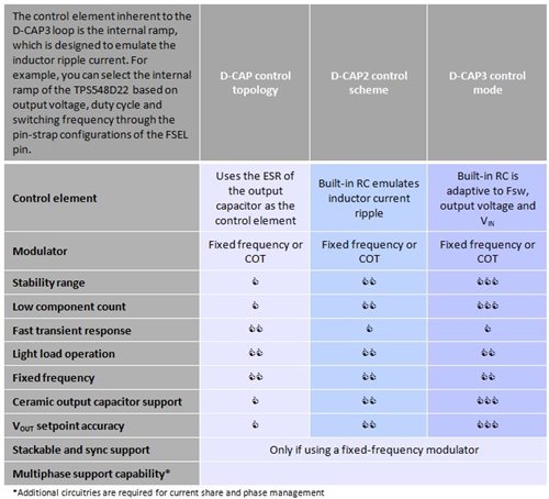
The first D-CAP controller was realized using an adaptive constant on-time (COT) modulator. Today, TI has a family of products using different modulators and evolving derivatives of the D-CAP control topology, such as the D-CAP2™ control scheme and D-CAP3 control mode. Figure 1 shows the evolution of the D-CAP family.
 Figure 1 D-CAP Family Evolution
Chart
Figure 1 D-CAP Family Evolution
ChartAfter several iterations, each improving upon the last, TI introduced the D-CAP3 control mode as an optimized D-CAP control loop with adaptive internal ramp compensation to support a wide range of external power-stage designs. In addition, the D-CAP3 control mode implements a ramp offset cancellation technique to improve VOUT setpoint accuracy performance. Unlike the D-CAP control topology, D-CAP3 control mode can stabilize almost any power-stage design using all multilayered ceramic capacitors (MLCCs), MLCCs plus bulk capacitors (with significant ESR) or bulk capacitor combinations. Table 1 below shows the general power supply considerations for the DCAP family of modulators.
|
The TPS548D22 works well with any output capacitor combination. In a typical TPS548D22 converter design, there are three primary considerations for selecting the value of the output capacitance: transient requirements, output voltage ripple and stability.
The TPS548D22 is a 40A converter, so for any given proper set of design constraints, the transient requirements generally dominate the output stage (output inductor and capacitor bank) design. A tight ripple specification (along with a tighter DC specification) is becoming critical in some high-end and high-performance application-specific integrated circuit (ASIC) and field-programmable gate array (FPGA) designs. In applications where accuracy is critical, you will need to design the output power stage to meet the ripple and DC criteria. There is a minimum capacitance requirement in terms of small-signal stability. This requirement is in place to prevent subharmonic multiple pulsing behavior in a COT modulator.
Generally speaking, if the converter is properly designed for both the transient and ripple requirements, the minimum capacitance requirement is considered satisfied, but you should still double-check the minimum capacitance requirement by using Equation 6 in the TPS548D22 data sheet.
In summary, D-CAP based control topology brings convenience to the power supply designer that is designing high performance POL converters. Consider TI’s SWIFT™ TPS548D22 synchronous step-down converter for your next design.