SSZTAM1 november 2016 TPS659037 , TPS65916
Hardware engineers often don’t consider the placement of the sense connection of buck converters in a power-management integrated circuit (PMIC) when powering an application processor. You might be thinking, “The sense pin for a buck converter must be connected to the output. What is there to consider?” Well, many application processors use voltage scaling to minimize the supply voltage in order to reduce power consumption and junction temperature. Minimizing the supply voltage requires a tight voltage tolerance in order to provide the lowest possible supply voltage, and one such voltage tolerance to consider is the I*R drop of the supply current through the printed circuit board PCB trace.
For example, a 2-inch long trace up to 1-inch wide with 0.5oz copper on an evaluation board has about 8mΩ resistance. With a max load of 5A, there could be a drop of as much as 40mV from the PMIC output to the processor input. AM57xx processors provide a target voltage in 10mV steps, which is much smaller than this 40mV variation. So how do you improve this?
Any PCB trace must have resistance, so you can’t remove the I*R drop. But one solution is to route the buck sense pin to the load instead of to the buck output capacitor. If the PMIC is regulating to 1.2V, it will regulate the output voltage so that 1.2V is seen at the load regardless of the load current. A good place to route the sense connection is to one of the bulk capacitors, getting as close as possible to the processor supply pin.
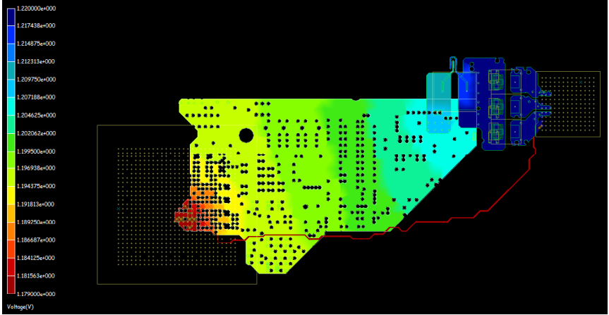
Figure 1 shows an example layout using remote sensing on the buck using the example numbers above. The trace resistance is about 8mΩ and the load current is 5A, giving a 40mV drop from the PMIC output to the processor supply pins. Because the sense voltage is routed to the processor, the PMIC is regulating its target 1.18V at the load, as seen by the red color on the feedback line in Figure 1.
 Figure 1 PMIC Power Trace and Remote
Sense Connection (Red). the Voltage Gradient Goes from Blue (Higher Voltage) to
Red (Lower Voltage)
Figure 1 PMIC Power Trace and Remote
Sense Connection (Red). the Voltage Gradient Goes from Blue (Higher Voltage) to
Red (Lower Voltage)When routing the sense pin across the board, you need to shield it from noise. Make sure to route the sense line away from other switching lines on the board. I also recommend shielding the sense lines with power or ground planes above and below. If the regulator has differential sensing – meaning that it has a sense output and a sense ground line – route the two lines in parallel in order to reduce common-mode noise. Figure 2 shows an example of differential feedback routing using the TPS659037 regulator SMPS12.
 Figure 2 Differential Routing Feedback
Showing Output Voltage Feedback (Red), Ground Feedback (Orange) and Package
Outline (White)
Figure 2 Differential Routing Feedback
Showing Output Voltage Feedback (Red), Ground Feedback (Orange) and Package
Outline (White)Sense pin routing is only one aspect of layout guidelines for a PMIC. For more layout guidelines, see the layout section of the device data sheet. Also check out TI’s PMIC selection for more ways to power your application processor.
Additional Resources
- Read through the TPS659037 layout guidelines.
- Look at Power and Thermal Design Considerations for TI’s AM57x Processor