SSZTAS7 october 2016 ISO7831 , LMG3410R070 , UCD3138
As a power electronics engineer, there is a saying that no success is made without the lessons learned from power devices blowing up. This seemed true during my years of experience debugging switched-mode power supplies with silicon-based MOSFETs. It is through trial and error and the study of device failures that you learn how to design a converter that works reliably.
In the early stages of gallium nitride (GaN) power FETs, failures were common. More stringent gate-loop design requirements, much higher dv/dt and the effect of common-source inductance all made the circuit much more sensitive to parasitics and noise. When TI’s first 600V GaN power stage samples came out, I marveled at the product’s robustness and the effectiveness of its self-protection functions. Even though the power stage had been validated through rigorous testing, my previous experience with silicon parts left me curious of its robustness under actual usage. More importantly, will these functions change the conventional wisdom of circuit prototyping and debugging ?
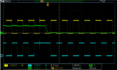
In a recent design of an interleaved converter, I used two TI half-bridge LMG3410-HB-EVM evaluation modules (EVMs) with some basic DC bus design, controlled by a UCD3138 digital pulse-width modulation (PWM) controller. When the two interleaved half bridges worked together, I saw that the PWM signal was repeatedly affected by high dv/dt (100V/ns), causing shoot-through across the FETs at 480V and triggering the integrated overcurrent protection (Figure 1).
Unlike the majority of FETs – which would fail in this situation – the LMG3410 integrated power stage enabled me to repeat the fault condition without damage, and to debug to the root cause quickly. This would have been very painstaking and possibly unsafe to do with traditional parts.
 Figure 1 Self-shutdown of the Power
Stage Following a Shoot-though Event (Blue: upper-FET PWM; Yellow: lower-FET
PWM; Green: Inductor Current)
Figure 1 Self-shutdown of the Power
Stage Following a Shoot-though Event (Blue: upper-FET PWM; Yellow: lower-FET
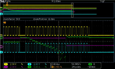
PWM; Green: Inductor Current)By varying the slew rate through RDRV, I found that 50V/ns or 100V/ns with single-phase operation had robust operation, while 100V/ns with two-phase operation did not. The root causes were contamination from common-mode (CM) noise and a nonoptimized layout of the controller’s peripheral circuits, resulting in a clock-synchronization mismatch across different PWM channels (Figure 2).
 Figure 2 PWM Out-of-sync Leads to
Inductor Current Surge (Blue: upper-FET PWM; Yellow: lower-FET PWM; Green:
Inductor Current; Red: Fault-signal Triggering)
Figure 2 PWM Out-of-sync Leads to
Inductor Current Surge (Blue: upper-FET PWM; Yellow: lower-FET PWM; Green:
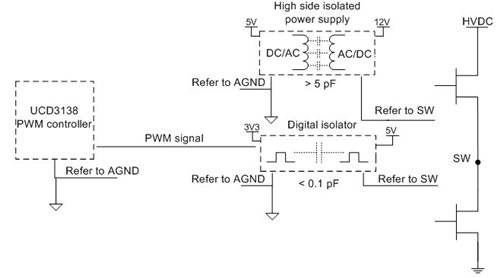
Inductor Current; Red: Fault-signal Triggering)TI’s ISO7831 digital signal isolator provides an adequately high CM transient immunity (CMTI) rate (>100V/ns), but the isolated power supply (which usually has much higher CM capacitance) would easily couple noise from the switching-node voltage to the control-side ground at high dv/dt (Figure 3). With multiple phases operating simultaneously, more CM noise would be injected into the control side.
Power-supply designers sometimes overlook this issue, since silicon devices and some GaN FETs with external drivers will not achieve such a high slew rate. I successfully resolved the issue by adding extra CM chokes on the upper FET’s isolated power supply and improving the decoupling loop of the digital controller, which reduced ground bouncing and noise coupling at the controller. Thanks to LMG3410’s integrated protection functions, I didn’t experience a single catastrophic failure during the whole debugging experience, despite repeated CM noise-induced faults.
 Figure 3 CM Capacitance across Isolated
Power Supply and Digital Isolator
Figure 3 CM Capacitance across Isolated
Power Supply and Digital IsolatorBesides overcurrent faults, overtemperature events are common occurrences in power converters. Although an experienced engineer has good thermal design skills, keeping the device junction cool is still challenging, and there is not much margin for error. Over time, events such as fan failures or heatsink deterioration can cause catastrophic failures. Fortunately, the LMG3410 has integrated overtemperature protection, and it came to my rescue when my fan’s power supply got turned off accidentally. The thermal trip point is set at 165°C, allowing enough margin for brief temperature excursions but preventing the device from suffering permanent damage due to cooling-related system failures.
While GaN brings advantages in system efficiency, size and cooling, its high switching speed and frequency also present increasing challenges. The protection and other integrated functions of TI GaN products are changing the conventional wisdom of using discrete Si MOSFETs for us to learn about the intricacies of high-speed switching-converter designs. These products not only protect the device against permanent damage as we debug our new designs, but also improve robustness by preventing gate overstress under long-term operation, since an integrated driver design reduces gate ringing.
The world has seen tremendous scaling of electronics and improvement of system density with Moore’s law. This trend is now coming to power electronics, thanks to the development of GaN technology and the introduction of easy-to-use GaN power stages like the LMG3410 with self-protection features.
Get to know TI’s GaN solutions.
Additional Resources:
- Let’s GaN together, reliably
- A comprehensive methodology to qualify the reliability of GaN products
- APEC 2016: Application-relevant Qualification of Emerging Semiconductor Power Devices
- IEEE International Reliability Physics Symposium 2016 (Invited paper): Product-level Reliability of GaN Devices