SSZTAW9 september 2016 TPD1E01B04 , TPD1E04U04 , TPD1E0B04 , TPD1E1B04 , TPD4E02B04
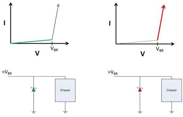
As technology continues to progress, many technology companies are focused on squeezing more and more chipsets into smaller spaces. As a result, chipsets have continued to shrink in size since the invention of the integrated circuit. As chipsets continue to shrink in size, they become more sensitive to unwelcome voltage transients such as electrostatic discharge (ESD). Although there are a variety of ESD protection devices, the method of protection is similar for each. The ESD transient voltage suppressor (TVS) diode is placed in parallel with the chipset. If the voltage on the node exceeds a certain threshold, the diode will conduct and protect the chipset (Figure 1).
 Figure 1 ESD Diode in the off State
(Left); ESD Diode in the on State and Conducting (Right)
Figure 1 ESD Diode in the off State
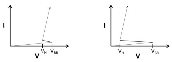
(Left); ESD Diode in the on State and Conducting (Right)Some ESD protection devices can exhibit a temporary negative resistance and “snap back” the voltage to a lower set voltage or holding voltage, VH. The difference between VH and the breakdown voltage can be small (shallow snap back) or quite large (deep snap back).Deep snap-back devices can offer the benefit of lower clamping voltages, but there is a risk. If you don’t consider certain design specifications, a phenomenon called data latch-up can occur. In the event of a sudden transient such as an ESD strike, the diode will snap back to VH (Figure 2). But if the VH of the device is within the working voltage range of the signals passing through, the diode could stay in the conducting “on” state even after the ESD strike has passed. This is known as latch-up and can be detrimental for a number of reasons.
The first reason is that ESD protection diodes are not designed to handle continuous conduction currents. Such currents could damage the protection diode, as well as the chipset the diode is supposed to protect. The second reason is that while the diode is conducting current, the voltage across the diode may be too low for the chipset to function. Since the diode and chipset are connected in parallel, if the diode is holding the voltage at a certain level, the chipset is also holding that voltage.
 Figure 2 Shallow Snap-back (Left); Deep
Snap-back (Right)
Figure 2 Shallow Snap-back (Left); Deep
Snap-back (Right)The deeper the snap back or the lower the holding voltage, the more likely latch-up will occur. To avoid this problem, you must consider several design considerations when using deep snap-back protection diodes, including the benefit of diode low clamping.
Low capacitance (CL) and low dynamic resistance (RDYN) also need to be considered when choosing a protection diode. The increase in data speeds in interfaces such as High-Definition Multimedia Interface (HDMI) 2.0 and USB 3.1 present a need for ESD diodes with CL as well as RDYN. Having a lower CL maintains signal integrity and supports faster data rates, while a lower RDYN allows for a lower clamping voltage. Generally, the relationship between CL and RDYN is inversely related: lowering one would increase the other. However, TI’s new ESD diodes have both low CL as well as low RDYN. The diodes also have shallow snap back with low clamping voltages, which removes the risk of latch-up. Table 1 highlights diode a few specifications of these diodes.
| TI part number | Interface | Capacitance (CL) | Dynamic resistance (RDYN) | Breakdown voltage (VBR) |
| TPD1E0B04 | Antenna, Thunderbolt 3 | 0.13pF | 1Ω | 6.7V |
| TPD1E01B04 | USB Type-C™, Thunderbolt 3 | 0.18pF | 0.6Ω | 6.4V |
| TPD1E04U04 | USB 3.0, HDMI 2.0/1.4 | 0.5pF | 0.2Ω | 6.2V |
| TPD1E1B04 | USB, (General Purpose Input/Output GPIO, Pushbuttons | 1pF | 0.15Ω | 6.4V |
| TPD4E02B04 | USB Type-C, USB 3.1 Gen 2 | 0.3pF | 0.5Ω | 6.4V |
In summary, deep snap-back protection diodes offer the benefit of clamping at lower voltages. However, these diodes need to be implemented with several considerations. If these design considerations are not implemented correctly, then there is the risk of latch-up which could damage the protection diode, the chipset or both. However, a low capacitance, low RDYN protection diode provides the benefit of low clamping voltages without the risk of latch-up making it a simple, cheap solution for many interfaces.
Log in to leave a comment below or visit the TI E2E™ Community ESD/EMI forum to join others talking about protection devices.
Additional Resources
- Check out TI’s ESD protection products.
- Read the white paper, “Latch-Up,” for more information about complementary metal–oxide–semiconductor (CMOS) latch-up.
- Download these documents for more information about ESD protection: