SSZTBN9 February 2016 DS250DF810 , DS280BR810 , TPS53513
When transitioning from 10G to 25G for next-generation servers and switches, hardware design engineers have to satisfy competing objectives: minimize data latency, maintain or reduce power consumption, and keep costs as low as possible. You essentially need to do more with less in order to deliver first-rate products to your data-center customers at a competitive cost.
Here are five quick tips for designing your 25G system to strike the right balance:
-
Determine which links in the system will need signal conditioning; this will depend on routing length and printed circuit board (PCB) material. Low-loss material requires fewer signal conditioners but is more expensive compared to standard materials. Channels with loss greater than the application-specific integrated circuit’s (ASIC’s) inherent compensation capability will require some form of signal conditioning. For example, if your ASIC is capable of 30dB compensation, you will probably want to add signal conditioning to channels that have a 27dB loss or more, with the 3dB difference acting as your safety margin.
Figure 1 is an example channel-loss budget analysis comparing PCB materials A and B.
 Figure 1 Example
Distribution of Channels in a System Assuming ASIC Loss-compensation
Capability: 30dB at 12.9GHz, PCB Material a Loss: 0.8dB/inch at
12.9GHz, and PCB Material B Loss: 1.1dB/inch at 12.9GHz
Figure 1 Example
Distribution of Channels in a System Assuming ASIC Loss-compensation
Capability: 30dB at 12.9GHz, PCB Material a Loss: 0.8dB/inch at
12.9GHz, and PCB Material B Loss: 1.1dB/inch at 12.9GHz - For the channels that will require signal conditioning, design for flexibility by using a small footprint. A small footprint offers high channel density and allows you to use either a retimer or pin-compatible repeater.
- Design a power-supply solution that will accommodate either a retimer or a repeater. For example, the TPS53513 synchronous step-down converter can supply 8A, which is more than adequate for a grouping of six retimers or repeaters.
- Determine the SMBus address scheme needed to address each retimer/repeater device individually on the board. You can pin-strap each device with one of 16 unique SMBus addresses. If there are more than 16 devices on a board, consider using an I2C expander like the TCA/PCA family of I2C/SMBus switches to split the SMBus into multiple buses.
- Place a single low-cost 25MHz (±100ppm) 2.5V single-ended clock on the board to support up to 20 retimer devices. This clock does not have any jitter requirements, since its purpose is not to recover data. The retimer will take in the clock, buffer it and replicate it on an output pin for easy hookup to the next retimer. There’s no need to have multiple crystals or fanout buffers. If you ultimately decide to use repeaters instead, you can leave this component unpopulated to reduce cost.
To make following these tips easier, TI has introduced the industry’s first portfolio of pin-compatible repeater (DS280BR810) and retimer (DS250DF810) solutions enabling reach extension for 25G backplane and front-port applications. How does this help balance power, performance, and price? It’s all about design simplicity and flexibility.
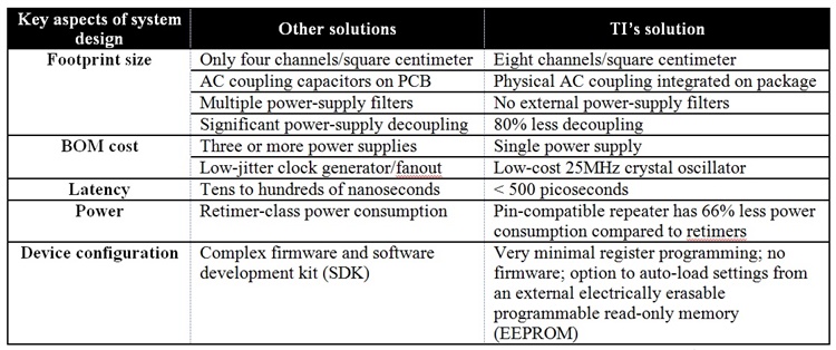
TI’s pin-compatible repeater and retimer solutions allow you to choose a solution that meets your performance targets while minimizing latency and reducing bill-of-materials (BOM) cost. Hardware engineers know that the cost, size, and complexity of surrounding components are just as important as the repeater or retimer itself. Consider Figure 2’s board design examples. versus a Generic Solution
(Left)") Figure 2 Illustrating the Simplicity
and Cost Savings of a TI Solution (Right) versus a Generic Solution
(Left)
Figure 2 Illustrating the Simplicity
and Cost Savings of a TI Solution (Right) versus a Generic Solution
(Left)
|
The pin-compatible nature of TI’s 25G DS280BR810 repeater and DS250DF810 retimer solutions allows you to generate one schematic to evaluate both options, enabling cost, power, and performance optimization for the final product. Signal integrity engineers can start testing with the repeater solution, which offers lower cost and reduced power consumption. They can upgrade to a pin-compatible retimer solution if the jitter and crosstalk in the system necessitates higher performance.
The small stuff really matters. Consider a typical data center consisting of 20,000 servers. Using a repeater instead of a retimer can save about 1W of power in a server network interface card (NIC), which can add up to over $21,000 in annual electricity savings ($0.12 per kilowatt hour), not including savings on cooling. If you eliminated $5 worth of components from the BOM, that translates to another $100,000 in savings. Finally, the difference between 50ns of latency versus 500ps can result in almost eight hours per day that would have been “wasted” while servicing requests across the whole data center (assuming 2,000 requests per second and four hours of total utilization time per server per day).
By following these tips, you should end up with a board design that allows you to strike a balance between cost, power, and performance.
Additional Resources
- Learn more about TI’s signal-conditioning portfolio.
- Download the DS280BR810 data sheet.
- Check out the DS250DF810 data sheet.
- Simplify design with the TI WEBENCH® Interface Designer tool.
- Watch a video demonstration of TI’s 25G retimer and repeater products.
- Download TI’s 100GbE QSFP28 reference design.