SSZTBO4 January 2016 MSP430F5132 , OPA374
Welcome back! If you missed part 1 of this series, I discussed the necessity of cycle-by-cycle over current protection in BLDC motor drives and how to sense the motor winding current. In part 2, I will discuss on how to implement the cycle-by-cycle over current protection by sensing the DC bus current and using an ultra-low power microcontroller.
TI’s ultra-low power MSP430F5132 microcontroller helps to control the motor-winding current on a PWM cycle-by-cycle basis without any software interrupt intervention.
 Figure 1-1 Cycle-by-cycle Current-limit
Implementation Using a Differential Amplifier and the MSP430F5132 MCU
Figure 1-1 Cycle-by-cycle Current-limit
Implementation Using a Differential Amplifier and the MSP430F5132 MCUYou can configure the high-bandwidth precision OPA374 as a single-ended differential amplifier to amplify the voltage drop across the sense resistor, RSENSE, connected in the DC bus return path
The MSP430F5132 MCU has an integrated comparator and timer event control (TEC) module that you can configure to implement the current limit. The comparator compares the analog voltages at the noninverting (+) and inverting (–) input terminals. If the noninverting terminal is more positive than the inverting terminal, the comparator output, CBOUT, is high.
You can use the output of the comparator with or without internal filtering. When setting the control bit, CBF, in the MCU, the output is filtered with an on-chip resistor-capacitor (RC) filter. You can adjust the delay of the filter in four different steps, which allows you to optimize the comparator’s response time. The output filter will suppress noise spikes, which can avoid false switching at the output of the comparator. The output filter can also reduce errors associated with comparator output oscillation when the voltage difference across the input terminals is small. The comparator features a high-precision reference voltage; to obtain different voltage references, configure the CBRSEL bit in the CBCTL2 register. The reference voltages available are 1.5V, 2.0V and 2.5V.
The TEC module is the interface between the timer modules and the external events. The TEC and Timer_D modules are connected through internal signals. The TEC module contains the control registers to configure the routing between TEC and timer modules. The TEC module also has the enable register bits, interrupt enable and interrupt flags for external event inputs. On receiving the external fault or clear signals, the TEC module controls the timer output and thus the PWM signal.
The COMPB module and TEC module are used together for cycle-by-cycle current-limit protection. You must externally route the output of the comparator, CBOUT, to the TECxFLT1 external fault event pin of the TEC module, as shown in Figure 1-2, for current-limit protection.
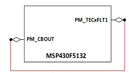 Figure 1-2 CBOUT Routed Externally to the
TECxFLT1 External Fault Event Pin
Figure 1-2 CBOUT Routed Externally to the
TECxFLT1 External Fault Event PinThe operation of the TEC module is shown in Figure 1-3. Whenever the current-sense differential amplifier output exceeds the voltage reference of the comparator, the output CBOUT and hence TECxFLT1 goes high, which initiates an event in the TEC module. The TEC module is programmed to disable the Timer_D output PWM during such an event. The Timer_D is configured in SET/RESET mode so that during the external event, the Timer_D resets and causes the PWM output pin to go low. This programmed function means that CBOUT goes high when the motor hits an overcurrent condition and can disable the Timer_D output (as Figure 1-3 shows) if CBOUT is connected to TECxFLT input pin. Figure 1-3 shows that the PWM turns off immediately when the comparator output goes high. When CBOUT goes low, the Timer_D output is then allowed to resume normal operation.
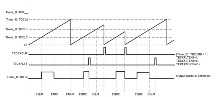 Figure 1-3 External Input Events
Resetting Timer_D Output
Figure 1-3 External Input Events
Resetting Timer_D OutputFigure 1-4 shows the current-limit operation when the comparator reference, VREF, is set at 1.5V, with a 60mΩ sense resistor (RSENSE) and a differential amplifier gain of 20.
The set over current limit (IOC_LIMIT) can be calculated using Equation 1.
Overcurrent limit, IOC_LIMIT = VREF/(RSENSE*amplifier gain) (1)
At VREF = 1.5V, IOC_LIMIT = 1.5 / (0.06*20) = 1.25A
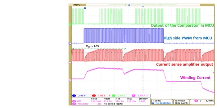 Figure 1-4 Cycle-by-cycle Current Limit
Using the MSP430F5132 MCU Hardware Features
Figure 1-4 Cycle-by-cycle Current Limit
Using the MSP430F5132 MCU Hardware FeaturesFigure 1-5 shows the response time of the comparator and TEC module with an external trip signal connected to the comparator input. The test results show that the time between the comparator input going more than 1.2V (to ensure the worst case, I considered a lower voltage compared to the 1.5V reference to calculate the response time) and the PWM shutdown is approximately 356ns. Therefore, the total response time of the current-limit action is less than 1µs. Figure 1-6 shows the response time from the comparator output going high to a PWM shutdown event, which is approximately 100ns. The test results show that the hardware features in the MCU ensures a very fast cycle-by-cycle current limit action and hence protects the motor drive.
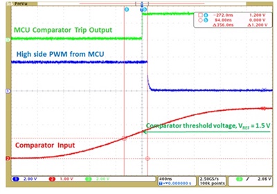 Figure 1-5 Total Response Time of the
Cycle-by-cycle Current-limit Protection
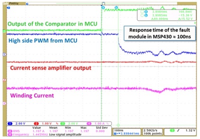 Figure 1-6 The Response Time from
When the Comparator Goes High to the PWM Shutdown
Figure 1-6 The Response Time from
When the Comparator Goes High to the PWM ShutdownThank you for reading this blog series. I hope you found it helpful in understanding necessity of cycle-by-cycle over current protection in BLDC motor drives and how we can implement this method of over current protection using an ultra-low power microcontroller.
Additional Resources
- Check out our TI Designs 230-V, 250-W, High Efficiency BLDC Motor Drive w/DC Bus Voltage Ripple Compensation Reference Design.
- To view more solutions to enable your motor control design, visit www.ti.com/motor.
- Learn more about the MSP430F5132 MCU.
- Read the application report “Sensored 3-Phase BLDC Motor Control Using MSP430” for more advice.