SSZTBO8 January 2016 TCAN332
Welcome to the third post in this series about the controller area network (CAN). In my last post, I focused on what CAN bus signals look like in terms of voltage levels on the bus pins. In this post, I’ll focus on the typical topology of the CAN driver output stage to drive those bus voltages. For anyone that has ever had emissions problems or output differential voltage problems in a CAN network, this blog describes how the driver works and what electrical parameters you can look at in a datasheet to identify a good transceiver. I believe a basic understanding of the CAN driver can also help aid with debugging CAN issues if they arise.
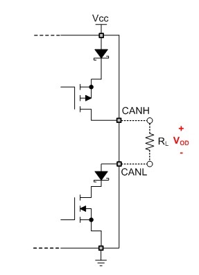
CAN transceivers like the TCAN332 usually have an equivalent two-output structure, as shown in Figure 1. The high-side output structure consists of a series diode and a P-channel transistor, while the low-side output structure consists of a series diode and an N-channel transistor. On the high-side, the series diode blocks current from flowing into VCC net if the CANH bus voltage exceeds VCC during any transients or common-mode disturbances. The series diode on the low-side blocks current from flowing out of ground to the CAN bus if the bus voltage drops below the transceiver’s local ground during transients and common-mode disturbances.
 Figure 1 Equivalent Output Schematic of
a CAN Transceiver
Figure 1 Equivalent Output Schematic of
a CAN TransceiverAccording to the ISO 11898 CAN standard, the two valid states for a CAN bus are the:
- Dominant state – a minimum 1.5V output differential voltage (VOD) into a 50-65Ω differential load (TXD = low).
- Recessive state – a maximum 50mV VOD into a 50-65Ω differential load (TXD = high).
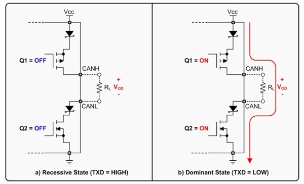
As shown in Figure 2, the driver is recessive when both the high- and low-side transistors are off and in a high impedance state. The driver is dominant when both the high- and low-side transistors are on and in a low impedance state.
 Figure 2 Recessive and Dominant
States
Figure 2 Recessive and Dominant
StatesSince both transistors are off in the recessive state (see the left side of Figure 2), negligible current will flow from VCC to ground. The VOD across the load resistance (RL) is very close to 0V. In the dominant state (the right side of Figure 2), both transistors are on and in a low impedance state. Therefore, current will flow from VCC to ground through the RL and create a VOD.
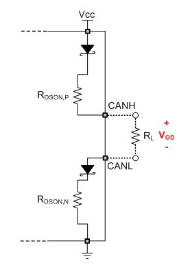
As I said in my previous blog, CANH and CANL are weakly biased to VCC/2 in the recessive state. To avoid creating common-mode disturbances when the device switches between recessive and dominant states, it is important to match the drive strength of CANH to VCC and CANL to ground. Looking at Figure 3, you can see that a well-matched drain-to-source on-state resistance (RDSON) of the P-channel and N-channel transistors centers the voltage drop across RL between VCC and GND at VCC/2.
If one half of the driver had a considerably lower on-state resistance than the other half, then the bus common-mode voltage would be pulled away from VCC/2 for the dominant state and back to VCC/2 for the recessive state. This would result in a shift of common-mode for every transition of bus states and therefore higher levels of conducted and radiated emissions.
 Figure 3 Equivalent Schematic Using
RDSON Resistor Values
Figure 3 Equivalent Schematic Using
RDSON Resistor ValuesWhen looking at driver electrical specifications, the two most important things to look for are the guaranteed output voltages for dominant and recessive states with a given load resistance (stronger drivers will guarantee output voltages with a lower resistance) and the driver symmetry between dominant and recessive states.
Now that you know what the output driver of a CAN transceiver looks like, stay tuned for my next post, which will describe a typical input-receiver topology. As always, feel free to post any comments or questions below.
Additional Resources
- Check out the new CAN bus transceivers page to see our products, support resources and technical documents.
- Explore the Polarity Correcting Isolated CAN Reference Design.
- See all the posts in the CAN blog series.