SSZTC43 september 2015 TMS320F28035
Power factor correction (PFC) systems are needed to take advantage of digital control techniques when working with power systems. The control loops of a power system are typically running at quick speeds to accommodate the fast switching frequency of the PFC power stage. Additionally, the complex switching patterns must be tightly controlled and modified at various points in the switching patterns.
Texas Instruments’ digitally controlled 2-Phase Interleaved Power Factor Correction (ILPFC) converter based on a single C2000™ TMS320F28035 microcontroller (MCU) has the capability of controlling a 700W interleaved PFC power stage. This kit is a reference design that can be modified to meet custom system requirements.
Let’s walk through how the software for this design is implemented.
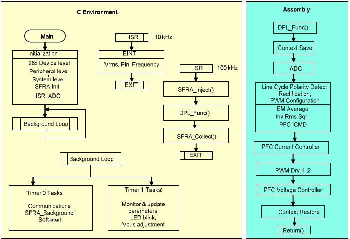
The software is comprised of functions written in both C and C-callable assembly. The C portion of the program consists of a main loop with two interrupt service routines (ISRs) running in the background. Several of the functions in the faster 100 kHz ISR are written in assembly for efficiency. The flow diagram for this design is shown in the diagram below:
This software structure remains the same for most PFC designs. Since this architecture remains similar and only the compensation coefficients for the compensator change, TI has designed a process for simplifying the software adaption for custom PFC board designs. The powerSUITE digital power software tools allow you to simply modify only a few PFC design parameters and generate the complete PFC code needed to meet your PFC system requirements. If your design requires use of different input or output voltages, different power stage component values, different digital controllers or a single-phase PFC topology, you can change these parameters on the Solution Adapter GUI.
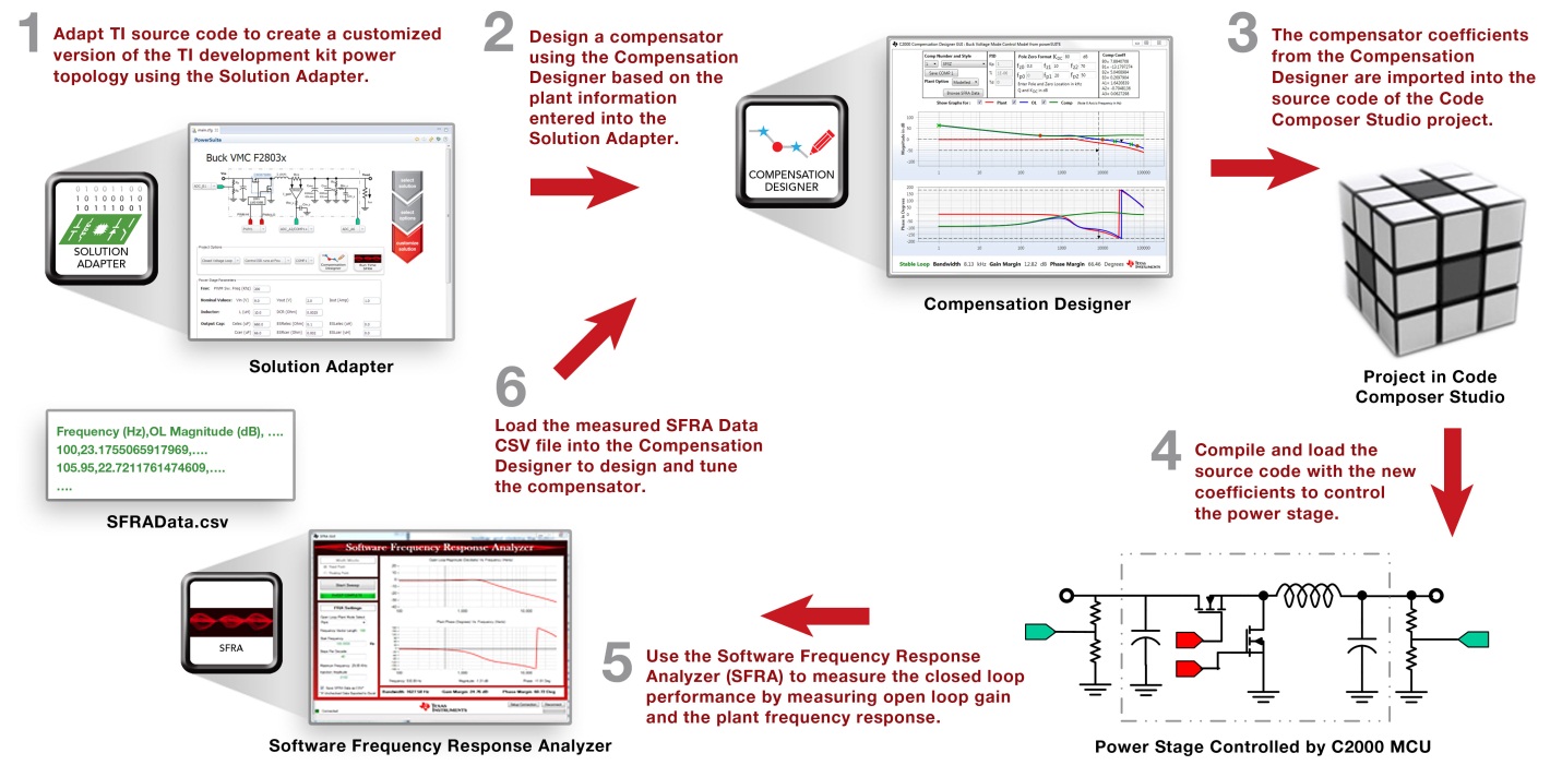
The values from the Solution Adapter GUI are used by the PFC power stage model in the Compensation Designer to plot the theoretical loop gain Bode plots for both the voltage and current loops of your custom PFC board. You can then modify the compensator values from this GUI to achieve the desired loop bandwidth, gain margin, and phase margin for both the voltage and current loops.
These theoretical values generated by the Compensation Designer can then be validated against the results from the Software Frequency Response Analyzer (SFRA). The data plotted by the SFRA is measured and calculated using the available processing capability in the C2000 MCU. This means that the frequency response is measured entirely in software on the MCU and then digitally transferred to the PC for viewing. However, this data could also be stored and analyzed by the MCU for on-chip system analysis. Once the actual frequency response has been measured and transmitted back to the PC running TI’s Code Composer Studio™ integrated development environment, the measured values of the power stage frequency response are used by the Compensation Designer to provide a more accurate, measurement-based Bode plot that can be used to more finely-tune the digital compensator to achieve the desired bandwidth, gain margin, and phase margin.
Why not try out this simplified design process yourself? Get started using the powerSUITE tools today with your own Power Factor Correction Design!
Login to your myTI account to leave a comment below with ways you can use the powerSUITE tools in your next design.