SSZTCX8 February 2024 LM5155 , LM5156
As useful as the rectification properties of diodes are, the forward voltage drop they create can vary widely with temperature. This increases losses and can introduce tolerance errors in power supplies.
While it may not be possible to eliminate their losses, it is possible to use diodes in ways that can reduce tolerance errors in certain applications. This article will provide three examples that will show you how to achieve this.
You can build a simple low-current voltage regulator from a resistor and a Zener diode. This type of regulator is often adequate for noncritical applications such as internal bias voltages. The circuit generally regulates the output voltage to about ±10% tolerance. However, it may be possible to improve the regulation by adding a diode in series.
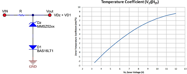
Figure 1 shows the addition of a diode in series with the Zener diode. The curve in Figure 1 plots the temperature coefficient for various Zener voltages. Above values of 4.7V, the temperature coefficient becomes increasingly positive, so as the operating temperature increases, the voltage across the Zener diode increases. If paired with the negative temperature coefficient of a diode, the increase of the Zener voltage will be offset in part by the decrease in the diode forward voltage, resulting in temperature error cancellation.
Zener values below 4.7V have a negative temperature coefficient, so adding a diode in series would actually increase regulation errors.
 Figure 1 A positive-temperature
coefficient Zener diode in series with a negative-temperature coefficient diode
can reduce temperature errors.
Figure 1 A positive-temperature
coefficient Zener diode in series with a negative-temperature coefficient diode
can reduce temperature errors.As an example, a 7.5V Zener diode shows a temperature coefficient of +5mV/° C, while a conventional diode (BAT16) is about −1.6mV/° C at 10mA. This value becomes increasingly more negative (−3mV/° C) with very small diode currents, so be sure to check it at the current level of the Zener diode. Ideally, the two temperature coefficients would perfectly cancel out, but that is not realistic or always necessary, as a simple improvement may be sufficient. For higher-voltage Zener diodes with even higher positive-temperature coefficients, two (or more) diodes could improve cancellation.
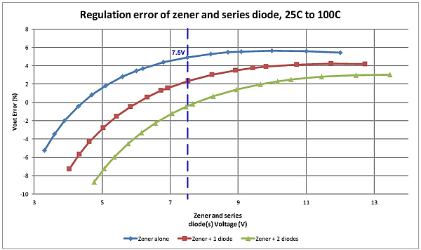
Figure 2 shows the calculated voltage regulation error of Figure 1 versus the output voltage for various Zener values – without series diodes, with one series diode and with two series diodes – operating between 25° C and 100° C. The vertical line in Figure 2 shows that adding series diodes can reduce temperature-dependent errors by 3-5% for a 7.5V output.
 Figure 2 Adding one or more diodes in
series with a Zener value over 4.7V reduces voltage regulation errors.
Figure 2 Adding one or more diodes in
series with a Zener value over 4.7V reduces voltage regulation errors.The second example involves converters that require a level shifter to send the output voltage information to the control circuit.
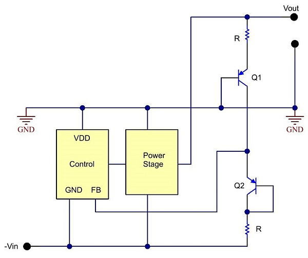
Figure 3 is a negative-input to positive-output inverting buck-boost. The control circuit is referenced to the −Vin rail, but the output voltage is referenced to GND. For the control circuit to accurately regulate the output voltage, the level shifter recreates the differential “Vout to GND” voltage between “FB and −Vin.” In this implementation, a current source approximately equal to (Vout − Vbe Q1 )/R flows from Vout to −Vin. This current flows in the lower resistor to reconstruct the output voltage referenced to −Vin. Adding Q2, configured as a diode, restores the Vbe drop lost from Q1. The level-shifted voltage at the FB pin now closely replicates that between Vout and GND, except for a small error related to beta.
One benefit of adding “diode” Q2 is that its forward voltage will be quite close to that of Q1, since almost the exact same current flows through both. To achieve the best voltage matching on Q2, you should use the same transistor as Q1. Another benefit is that both transistors have the same temperature coefficients, allowing their forward voltages to track each other more precisely. The temperature error associated with Vbe variations are significantly reduced since they cancel each other out (VFB ~ Vout −Vbe Q1 + Vbe Q2 ). It’s important to locate the Q1 and Q2 near each other so that they are exposed to the same temperature, or if possible, to use a dual-transistor package.
 Figure 3 A level shifter implements Q2
to cancel variations related to Q1.
Figure 3 A level shifter implements Q2
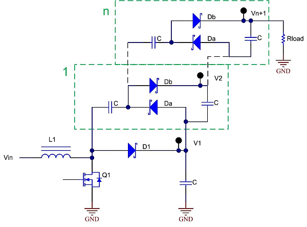
to cancel variations related to Q1.The third example shown in Figure 4 shows a boost converter with a series of charge-pump stages, where each stage “n” adds approximately “V1” to the total output at “Vn + 1.” For more details on voltage multiplier operation, see “Power Tips: Multiply your output voltage.”
 Figure 4 Charge-pump diode drops can
offset each other.
Figure 4 Charge-pump diode drops can
offset each other.Equation 1 approximates the total output voltage as:
From Equation 1, you can see that Vn + 1 is largely determined by multiples of n, but reduced by the “error terms” related to diode forward drops and the charge-pump transfer capacitor’s ripple voltage. Assuming that all diodes are the same type and that their forward voltages are equal:
VD1 = VDa = VDb, then Equation 2 is:
In Equation 2, the “error terms” on the right side reduce the output below its ideal n + 1 multiple. To improve this, using Schottky diodes for VDa and VDb and a conventional diode for VD1 , with forward voltage drops equal:
VDa = VDb = VD1 /2, then Equation 3 is:
From Equation 3, you can see that it is possible to reduce the error terms associated with the diode drops, thereby increasing the output voltage further. While Equation 3 is still an approximation, the concept is valid in that the output voltage will increase.
Diode forward voltage and temperature variations often degrade circuit performance, but that doesn’t always have to be the case. These design examples demonstrate methods in which it’s possible to cancel or minimize the temperature-dependent characteristics of diodes.
Check out TI’s Power Tips blog series on Power House.
Also see :
- Easily measure diode capacitance and reverse recovery
- Power Tips #79: Load transient testing with high slew rates
Previously published on EDN.com.