SWRA679 January 2021 CC3200 , CC3220R , CC3220S , CC3220SF , CC3230S , CC3230SF , CC3235S , CC3235SF
1.1 Basics of the SAR ADC Architecture
The Successive-Approximation Register Converter or the SAR ADC is essential to general-purpose mixed signal circuits. SAR ADCs are common in data acquisition applications such as power monitoring and low to medium frequency analysis. SAR ADCs offer moderate speeds of up to 4 mega samples per second while also offering medium to high resolutions with a high level of DC and AC accuracy. One of its most appealing advantages is the negligible to zero latency and low power consumption which makes it ideal for battery-powered applications. For most SAR ADCs power consumption is directly proportional to the sampling rates, so configurations at lower sampling rates allows for ultra-low power consumption.
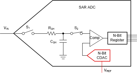
The SAR conversion process consists of two phases: The sampling phase and the conversion phase. During the sampling phase switch S2 opens and switch S1 closes. The analog input signal Vin then charges the sampling and hold capacitor CSH to the voltage level of the input. Once this acquisition phase is complete switch S1 opens and switch S2 closes, disconnecting the sample and hold capacitor from the external circuit. CSH is then connected to the internal comparator and the conversion phase begins.
 Figure 1-1 Simplified SAR ADC Internal
Architecture
Figure 1-1 Simplified SAR ADC Internal
ArchitectureThe N-bit search stack produces binary weighted analog voltages proportional to a reference as each bit decision is made in the binary weighted search. The binary search starts with the most significant bit decision and the tests are repeated for each binary weighted bit until the least significant bit decision is made. The value of each binary weight bit is based on whether the analog input signal is higher or lower than the DAC voltage. The successive approximation register provides the digital code to the internal DAC during each conversion clock cycle. The conversion time is a function of the conversion clock frequency and the resolution of the ADC. . Depending on the specific SAR ADC circuit, the initial voltage on a sample and hold capacitor during the next sampling phase may be reset to a midpoint voltage where it may keep value on the latest sample voltage. The device will trigger the next conversion after the next start conversion signal is received.
To learn more, see the TI Training: Choosing the Best ADC Architecture for Your Application.