SWRA679 January 2021 CC3200 , CC3220R , CC3220S , CC3220SF , CC3230S , CC3230SF , CC3235S , CC3235SF
2.1 Battery Voltage Measurements
The most obvious way to think about an ADC is to picture it as a multimeter. Apply an input voltage to the pin , configure the ADC to read the pin, read the output register and then convert it to an equivalent voltage using the expression V = code * Vref/2^N where, Vref is the reference voltage(1.467V), N is the number of bits (N = 12) and code refers to the output of the ADC read back from the internal register. Note that the bits 13:2 are the actual ADC codes.
Though this assumption is true to some extent, there are some pitfalls.
- The multimeter offers a high impedance input under all conditions whereas the ADC does draw current from the input.
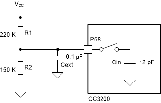
- The multimeter does some averaging on the input signal, whereas, the ADC is a spot measurement. These two characters make the ADC a bit difficult to work with. Figure 2-1 shows the recommended example for using our ADC to measure DC voltage.
 Figure 2-1 ADC Configuration
With the above circuit, the external capacitor gets charged to 1.34 V through the resistor divider while the ADC is not connected to the pin. When the ADC is connected to the pin, the internal capacitor starts to charge from the external capacitor. Since the switch resistance is negligible and the external capacitor is quite large compared to the internal one, the 12 pF cap can charge to the final value of 1.34 V.
The external capacitor is calculated based on the following calculation. Assuming that the Cin is charged from Cext fully, this will result in a charge re-distribution. Assuming that the entire charge is supplied from the Cext, we should not let the Cext voltage drop below 1LSB of the ADC. So the following can be calculated:
Cext = Cin x 4096, which gives 50 nF. For margin, it can be assumed that 2x the calculated value and use 100 nF (0.1 μF).
For more instructions on how to run this example, see the CC32xx SDK and the ADC single channel example.