SWRA749 September 2022
1.1 Required Voltage Rail and Signal Sequence
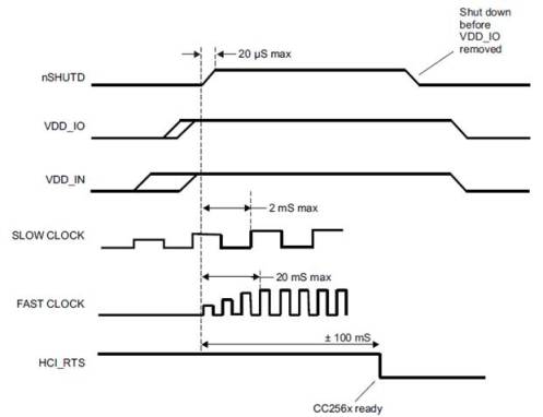
Proper power up of the device:
- nSHUTDOWN must be low.
- Turn on power supplies:
- Turn on VDD_IN (3.3V, max range is 1.8V to 4.8V)
- Turn on VDD_IO (1.8V, max range is 1.62V to 1.92V)
- VDD_IO and VDD_IN must be stable before releasing nSHUTDOWN.
- Slow Clock must be stable within 2ms of releasing nSHUTDOWN.
- Fast Clock must be stable within 20ms of releasing nSHUTDOWN.
- The CC256x device will indicate a complete proper power-up sequence by pulling HCI_RTS low.
 Figure 1-1 Proper Power Up Sequence
No signals are allowed on the I/O pins if VDD_IO power is not present. The only exceptions on this are the SLOW_CLK, XTALP, XTALM, and AUD_xxx pins that are fail-safe and can tolerate external voltages without VDD_IO and VDD_IN present.