TIDT240 October   2021


  1. 1Description
  2. 2Test Prerequisites
    1. 2.1 Voltage and Current Requirements
    2. 2.2 Required Equipment
    3. 2.3 Considerations
    4. 2.4 Dimensions
    5. 2.5 Signal Descriptions
  3. 3Testing and Results
    1. 3.1 Efficiency Graphs
    2. 3.2 Efficiency Data
    3. 3.3 Voltage Regulation Graphs
    4. 3.4 Cross-Loading Performance
    5. 3.5 Cross-Loading Performance Data
  4. 4Waveforms
    1. 4.1 Switching
    2. 4.2 Output Voltage Ripple
    3. 4.3 Load Transients
    4. 4.4 Start-up Sequence

Switching

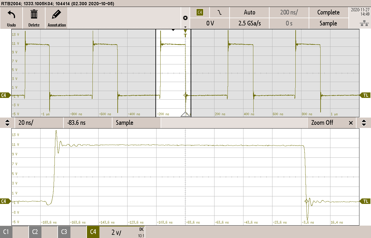
Figure 4-1 shows the LMR501410-Q1 switch node at 50% of nominal load.
GUID-20210722-CA0I-BWL2-CXPJ-JRSQZXZDV491-low.png
CH1 - pin 3
Figure 4-1 LMR50410-Q1 Switch Node

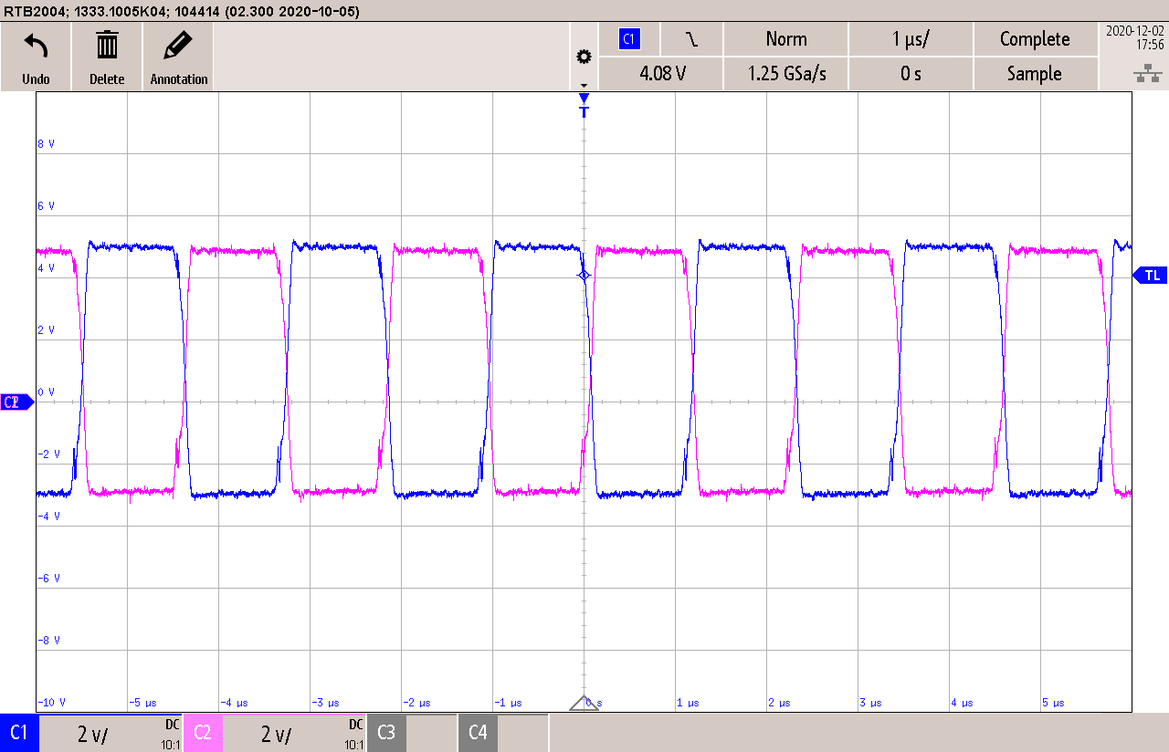
Figure 4-2 shows the output ripple VOUT1 with 330-Ω resistive load.
GUID-20210722-CA0I-C4RH-GWFX-VGLHKSLTGVD8-low.png
CH1 - pin 1, CH2 - pin 3
Figure 4-2 SN6505-Q1 Switch Node