TIDT240 October 2021
4.2 Output Voltage Ripple
Output voltage ripple measurements use the proper ripple-measurement technique that minimizes the voltage probe grounding loop. The oscilloscope uses the 20-MHz bandwidth limit.
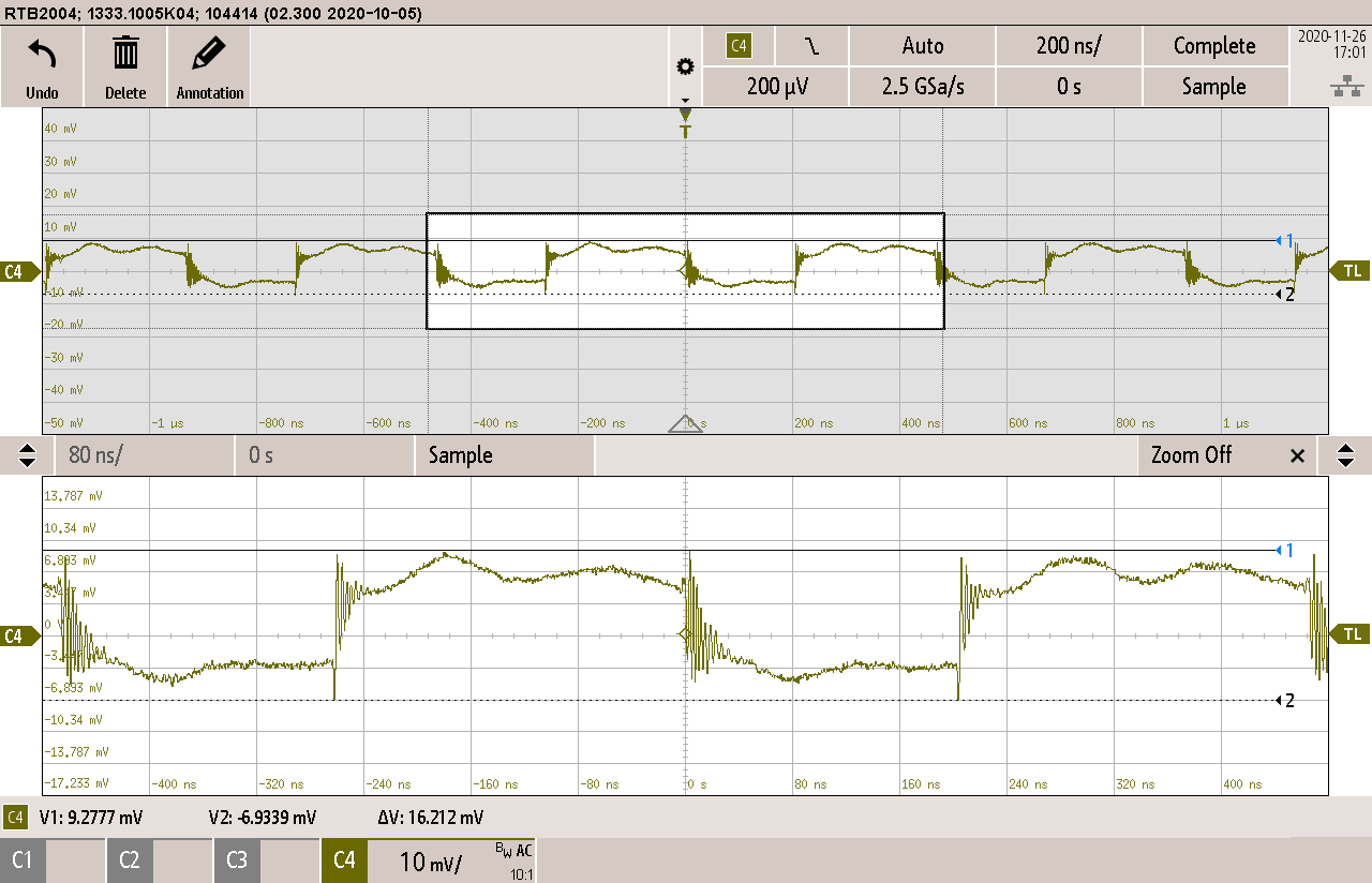
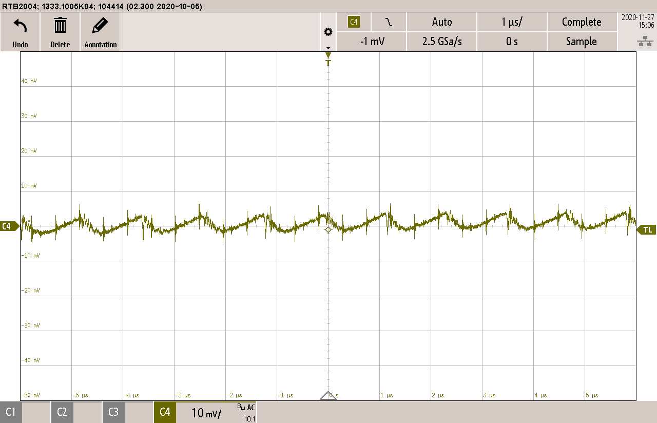
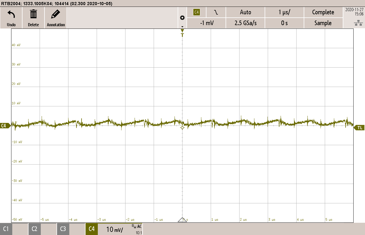
In Figure 4-3, the SN6505-Q1 is not assembled. Figure 4-4 shows the output ripple VOUT1 with 165-Ω resistive load. Figure 4-5 shows the output ripple VOUT1 with 330-Ω resistive load.
 Figure 4-3 LMR50410-Q1 Output Voltage
Ripple in CCM Mode
 Figure 4-4 SN6505-Q1 Output Voltage
Ripple
 Figure 4-5 SN6505-Q1 Output Voltage
Ripple