TIDT274 April   2022


  1.   Description
  2.   Features
  3.   Applications
  4. 1Test Prerequisites
    1. 1.1 Voltage and Current Requirements
    2. 1.2 Considerations
    3. 1.3 Dimensions
  5. 2Testing and Results
    1. 2.1 Efficiency Graphs
    2. 2.2 Load Regulation
    3. 2.3 Thermal Images
    4. 2.4 Bode Plots
  6. 3Waveforms
    1. 3.1 Switching
      1. 3.1.1 Switchnode to GND
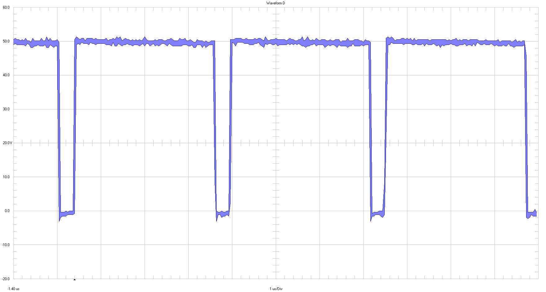
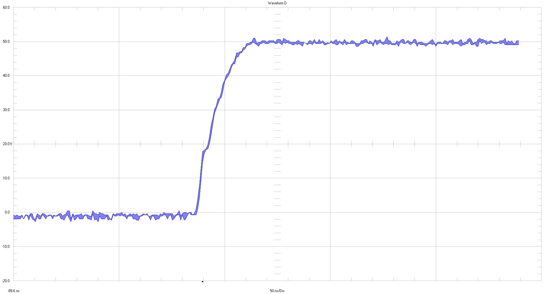
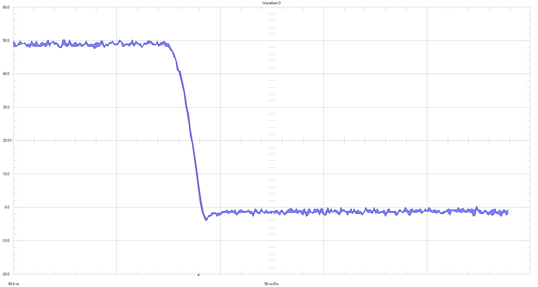
      2. 3.1.2 Switchnode to –VOUT
    2. 3.2 Input Voltage Ripple
    3. 3.3 Output Voltage Ripple
    4. 3.4 Load Transients
    5. 3.5 Start-Up Sequence
    6. 3.6 Shutdown Sequence

Switchnode to –VOUT

GUID-20220401-SS0I-DJVB-WQC4-XKWTPZDZJ5B5-low.jpg

10 V / div

1 µs / div

full bandwidth

GUID-20220401-SS0I-ZXFC-3SKP-SLFSSDG5FQJD-low.jpg
GUID-20220401-SS0I-QK13-XVPC-C1PG7ZBG8CS9-low.jpg

10 V / div

50 ns / major div

full bandwidth

The waveforms do not show any ringing and no overshoot.
Figure 3-2 Switchnode to –VOUT