TIDT280 May   2022


  1.   Description
  2.   Features
  3.   Applications
  4. 1Test Prerequisites
    1. 1.1 Voltage and Current Requirements
    2. 1.2 Considerations
    3. 1.3 Dimensions
  5. 2Testing and Results
    1. 2.1 Efficiency
    2. 2.2 Loss
    3. 2.3 Load Regulation
    4. 2.4 Line Regulation
    5. 2.5 Thermal Images
    6. 2.6 Bode Plots
      1. 2.6.1 9-V Input Voltage
      2. 2.6.2 24-V Input Voltage
      3. 2.6.3 48-V Input Voltage
      4. 2.6.4 56-V Input Voltage
  6. 3Waveforms
    1. 3.1 Switching
      1. 3.1.1 Transistor Q5 (Low-Side FET)
        1. 3.1.1.1 Drain - Source
          1. 3.1.1.1.1 9-V Input Voltage
          2. 3.1.1.1.2 56-V Input Voltage
        2. 3.1.1.2 Gate - Source
          1. 3.1.1.2.1 9-V Input Voltage
          2. 3.1.1.2.2 56-V Input Voltage
      2. 3.1.2 Transistor Q1 (High-Side FET)
        1. 3.1.2.1 Source - Drain (Referenced to VIN)
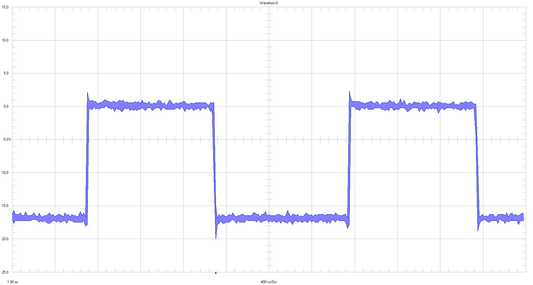
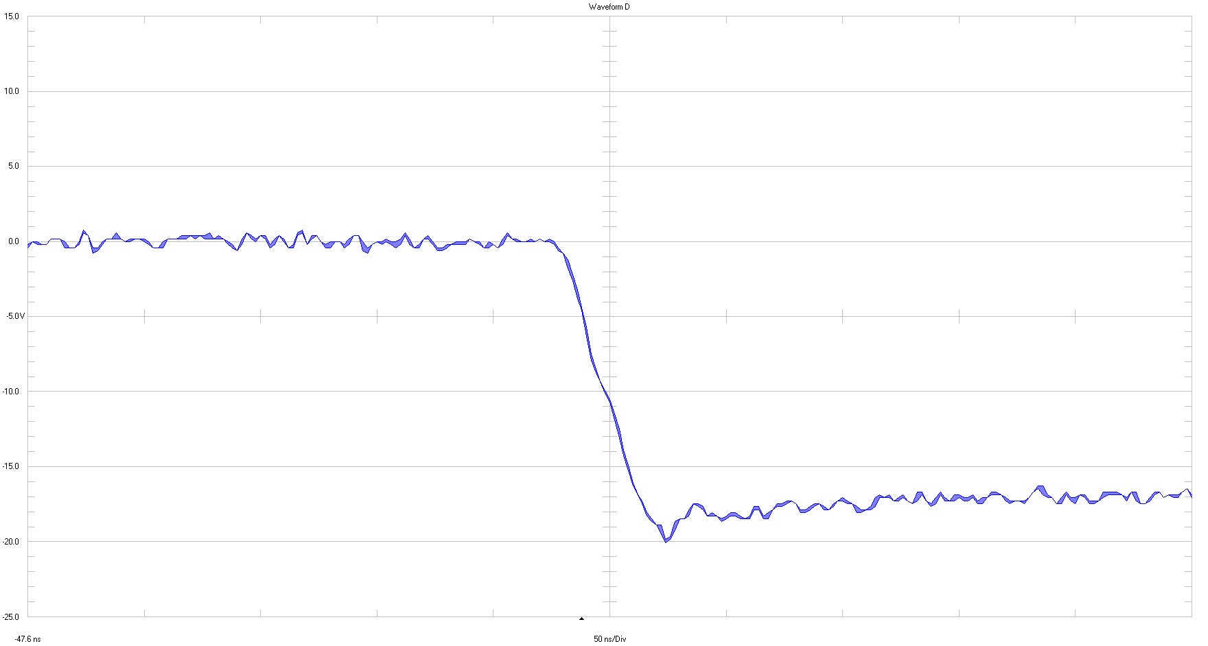
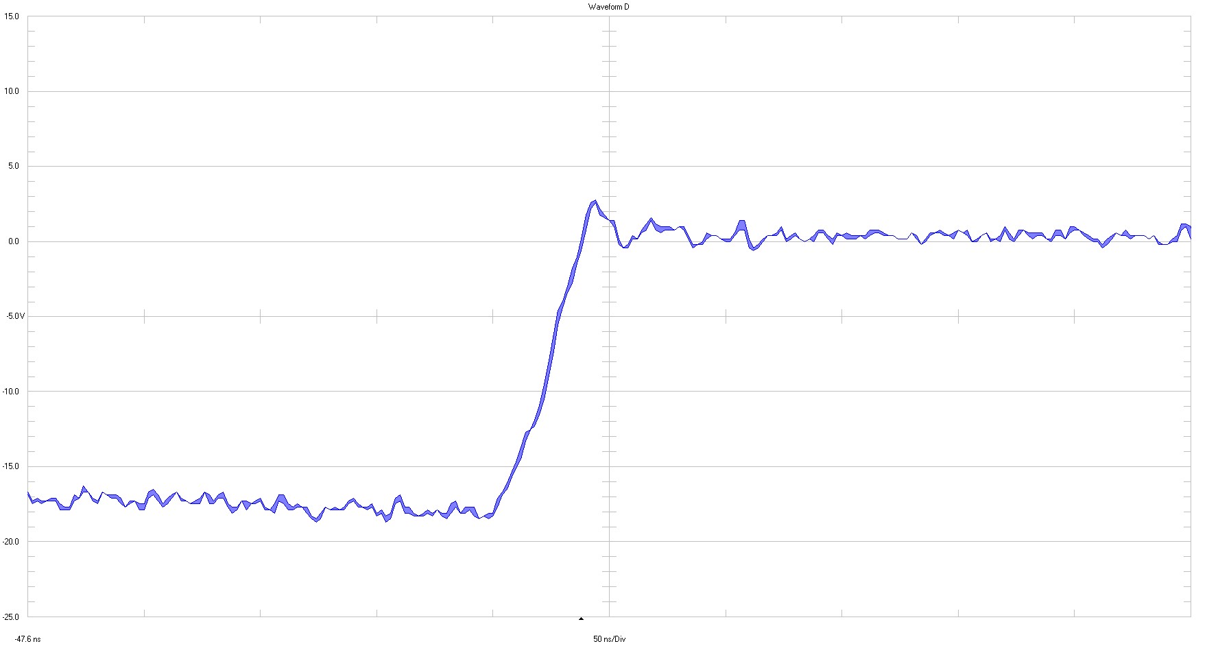
          1. 3.1.2.1.1 9-V Input Voltage
          2. 3.1.2.1.2 56-V Input Voltage
        2. 3.1.2.2 Gate - Source
          1. 3.1.2.2.1 9-V Input Voltage
          2. 3.1.2.2.2 56-V Input Voltage
    2. 3.2 Output Voltage Ripple
    3. 3.3 Input Voltage Ripple
    4. 3.4 Load Transients
      1. 3.4.1 9-V Input Voltage
      2. 3.4.2 56-V Input Voltage
    5. 3.5 Start-Up Sequence
      1. 3.5.1 9-V Input Voltage
      2. 3.5.2 56-V Input Voltage
    6. 3.6 Shutdown Sequence
      1. 3.6.1 9-V Input Voltage
      2. 3.6.2 56-V Input Voltage
9-V Input Voltage
GUID-20220422-SS0I-BD3P-PDD2-GF92LBDQ00TG-low.jpg

5 V / div

full bandwidth

400 ns / div

GUID-20220422-SS0I-MLRW-ZTVC-GHV8JWBJSHL9-low.jpg
GUID-20220422-SS0I-GM9R-66CL-BPRLBL1ZTDDD-low.jpg

5 V / div

full bandwidth

50 ns / major div

Figure 3-5 Q1 Source-Drain at 9 VIN