TIDT280 May   2022


  1.   Description
  2.   Features
  3.   Applications
  4. 1Test Prerequisites
    1. 1.1 Voltage and Current Requirements
    2. 1.2 Considerations
    3. 1.3 Dimensions
  5. 2Testing and Results
    1. 2.1 Efficiency
    2. 2.2 Loss
    3. 2.3 Load Regulation
    4. 2.4 Line Regulation
    5. 2.5 Thermal Images
    6. 2.6 Bode Plots
      1. 2.6.1 9-V Input Voltage
      2. 2.6.2 24-V Input Voltage
      3. 2.6.3 48-V Input Voltage
      4. 2.6.4 56-V Input Voltage
  6. 3Waveforms
    1. 3.1 Switching
      1. 3.1.1 Transistor Q5 (Low-Side FET)
        1. 3.1.1.1 Drain - Source
          1. 3.1.1.1.1 9-V Input Voltage
          2. 3.1.1.1.2 56-V Input Voltage
        2. 3.1.1.2 Gate - Source
          1. 3.1.1.2.1 9-V Input Voltage
          2. 3.1.1.2.2 56-V Input Voltage
      2. 3.1.2 Transistor Q1 (High-Side FET)
        1. 3.1.2.1 Source - Drain (Referenced to VIN)
          1. 3.1.2.1.1 9-V Input Voltage
          2. 3.1.2.1.2 56-V Input Voltage
        2. 3.1.2.2 Gate - Source
          1. 3.1.2.2.1 9-V Input Voltage
          2. 3.1.2.2.2 56-V Input Voltage
    2. 3.2 Output Voltage Ripple
    3. 3.3 Input Voltage Ripple
    4. 3.4 Load Transients
      1. 3.4.1 9-V Input Voltage
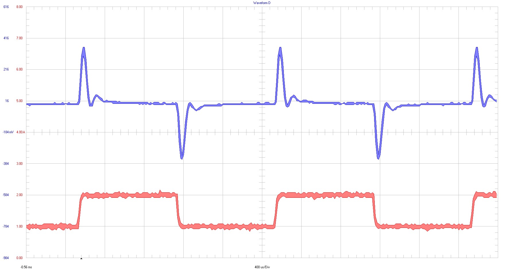
      2. 3.4.2 56-V Input Voltage
    5. 3.5 Start-Up Sequence
      1. 3.5.1 9-V Input Voltage
      2. 3.5.2 56-V Input Voltage
    6. 3.6 Shutdown Sequence
      1. 3.6.1 9-V Input Voltage
      2. 3.6.2 56-V Input Voltage

56-V Input Voltage

GUID-20220422-SS0I-LQV5-W9X4-DHQRXKQNJFW6-low.jpg

Ch1 ⇒ VOUT (AC)

200 mV / div

10-kHz bandwidth


Ch2 ⇒ IOUT

1 A / div

20-MHz bandwidth


400 µs / div

Figure 3-12 Load Transient 1 A to 2 A at 56-V Input Voltage