TIDT291 June 2022
2.3 Thermal Images
Thermal image are shown in the following figures.
All images were taken after running the supply at maximum load for 30 minutes. The board was mounted horizontally in open air at an ambient temp of 21°C with no additional air flow.
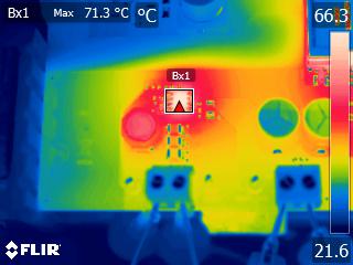
Bx1 – IC (U6)
Figure 2-3 Buck: 24-V Input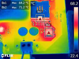
Bx1 – Diode (D2)
Bx2 – Transformer (T1)
Figure 2-5 Flyback Secondary: 24-V
InputBx2 – Transformer (T1)
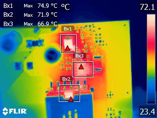
Bx1 – TVS Clamp (D3)
Bx2 – Transformer (T1)
Bx3 – Primary FET (Q3)
Figure 2-7 Flyback Primary: 10-V
InputBx2 – Transformer (T1)
Bx3 – Primary FET (Q3)
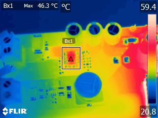
Bx1 – eFuse (U1)
Figure 2-9 Input Protection: 10-V
Input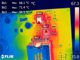
Bx1 – TVS Clamp (D3)
Bx2 – Transformer (T1)
Bx3 – Primary FET (Q3)
Figure 2-4 Flyback Primary: 24-V
InputBx2 – Transformer (T1)
Bx3 – Primary FET (Q3)
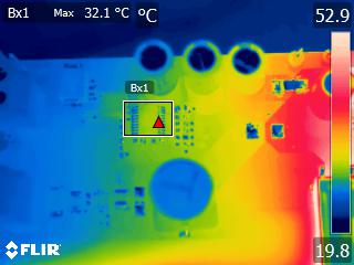
Bx1 – eFuse (U1)
Figure 2-6 Input Protection: 24-V
Input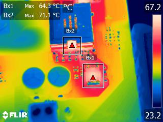
Bx1 – Diode (D2)
Bx2 – Transformer (T1)
Figure 2-8 Flyback Secondary: 10-V
InputBx2 – Transformer (T1)
