TIDT295 August 2022
3.1 Start-up Waveforms
Switching behavior is shown in the following figures. The waveform channel key is as follows: Light Blue: VBUS, Pink: VBAT, Green: Iout.
Figure 3-1 through Figure 3-4 illustrate the charge mode start up.
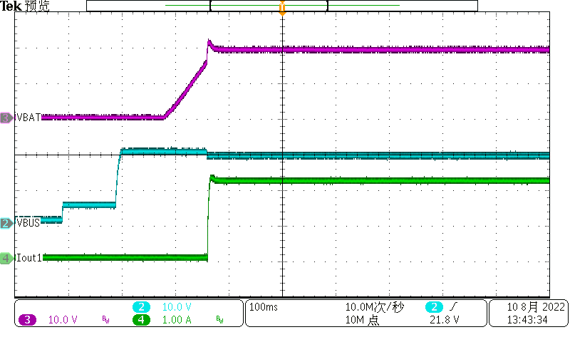 Figure 3-1 VBUS 20 V to VBAT 20-V Charge Mode
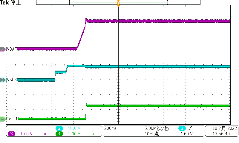 Figure 3-3 VBUS 9 V to VBAT 20-V Charge Mode
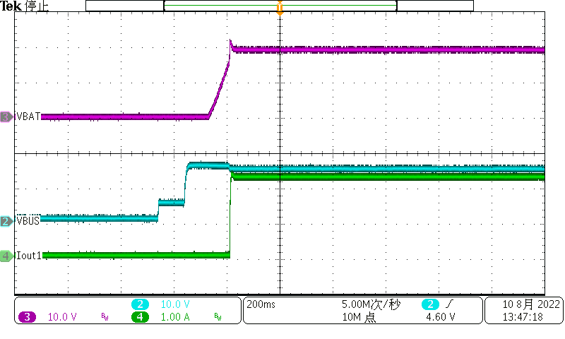 Figure 3-2 VBUS 15 V to VBAT 20-V Charge Mode
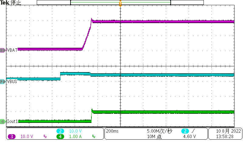 Figure 3-4 VBUS 5 V to VBAT 20-V Charge Mode
Figure 3-5 through Figure 3-8 illustrate OTG mode start up.
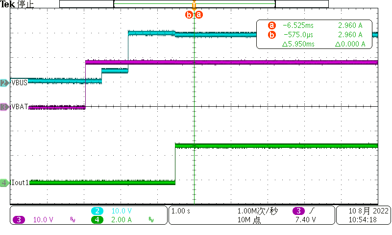 Figure 3-5 18 VBAT to 20 V, 3 A Out OTG Mode
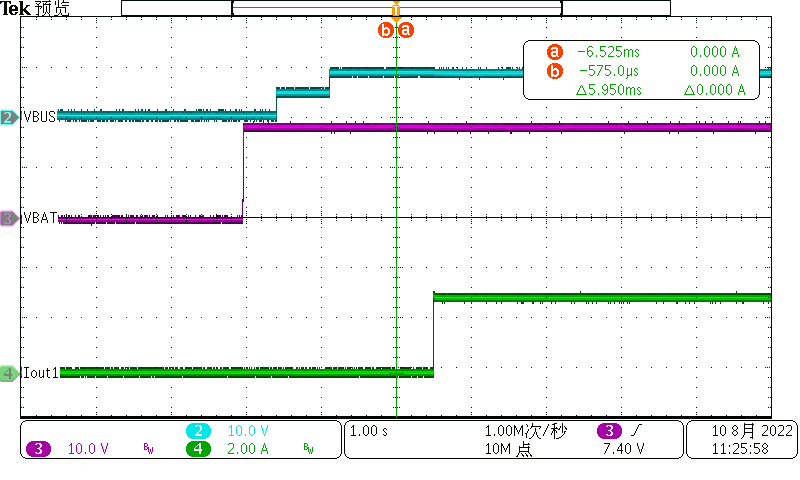 Figure 3-7 18 VBAT to 9 V, 3 A Out OTG Mode
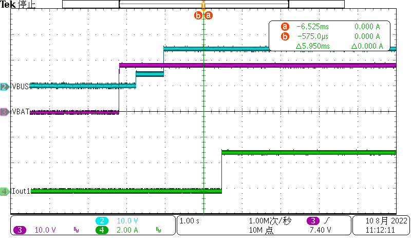 Figure 3-6 18 VBAT to 15 V, 3 A Out OTG Mode
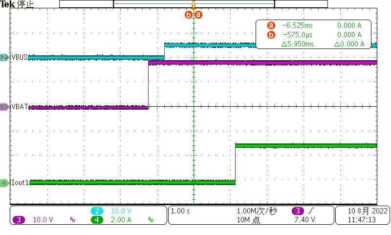 Figure 3-8 18 VBAT to 5 V, 3 A Out OTG Mode