TIDT320A january 2023 – july 2023
2.1 Switching Frequency and Operating Modes
The UCC28782 device has several operating modes that are dependent on the loading conditions. These different operating modes are optimized to provide high efficiency across the entire load range. A brief description of the different operating modes is provided here, along with associated waveforms measured on this reference design. For more details, see the UCC28782 High-Density Active-Clamp Flyback Controller with EMI Dithering, X-Cap Discharge, and Bias Power Management data sheet.
At maximum load, the UCC28782 is operating in Adaptive Amplitude Modulation (AAM) mode. In this mode, the converter is basically in transition mode and provides ZVS on every switching cycle.
As the load is decreased in AAM, the switching frequency increases due to the transition mode of operation. Once the frequency reaches a programmed maximum frequency, the converter enters Adaptive Burst Mode (ABM) operation. In ABM, the switching frequency remain fixed, and is sub-modulated at a lower burst frequency. In ABM, the first pulse in a burst packet is non-ZVS, but all other switching pulses are ZVS.
As the load is decreased in ABM, the number of switching pulses per burst packet are reduced to keep the burst frequency from entering the audible range. Once the number of pulses reaches two per packet, a further reduction in load causes the converter to enter Low Power Mode (LPM). In LPM, the active clamp switch is disabled to save power consumption, the number of pulses per burst packet is fixed at two, and the peak current is reduced. The reduction in peak current causes the switching frequency to increase as the load is decreased.
As the load continues to decrease in LPM, once the switching frequency reaches another clamping level, the converter enters Standby Power 1 (SBP1) mode of operation. In SBP1, the peak current once again becomes fixed, the number of pulses are fixed at two per burst packet, and the burst frequency is allowed to reduce lower.
At near-no-load operation, the converter transitions from SBP1 to Standby Power 2 (SBP2) mode of operation. In SBP2 mode, the number of pulses per burst packet is increased to four, and the peak current is increased. This allows the converter to operate at extremely low burst frequencies to minimize the no load power consumption.
In all the following figures, the input voltage was 390 VDC, and no load was applied to P18V and S12V.
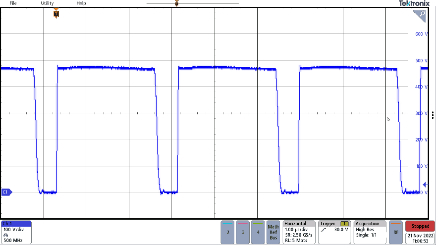 Figure 2-1 Primary Switch Node
Voltage in AAM (3.7 A on 12VSB)
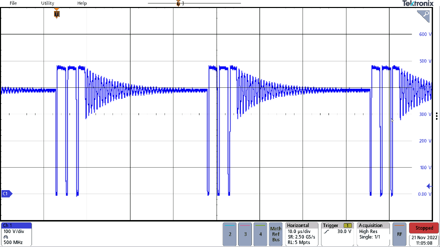 Figure 2-3 Primary Switch Node
Voltage in ABM, Near LPM-ABM Boundary (600 mA on 12VSB)
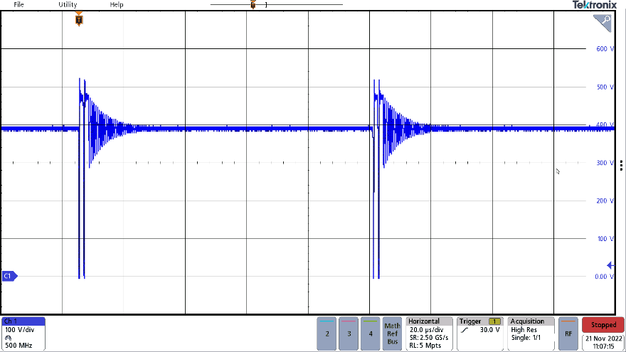 Figure 2-5 Primary Switch Node
Voltage in SBP1 (100 mA on 12VSB)
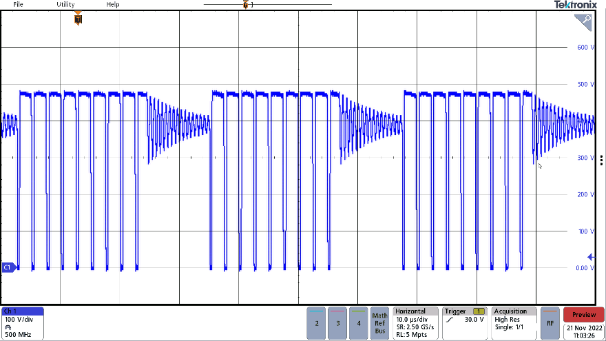 Figure 2-2 Primary Switch Node
Voltage in ABM, Near ABM-AAM Boundary (2.0 A on 12VSB)
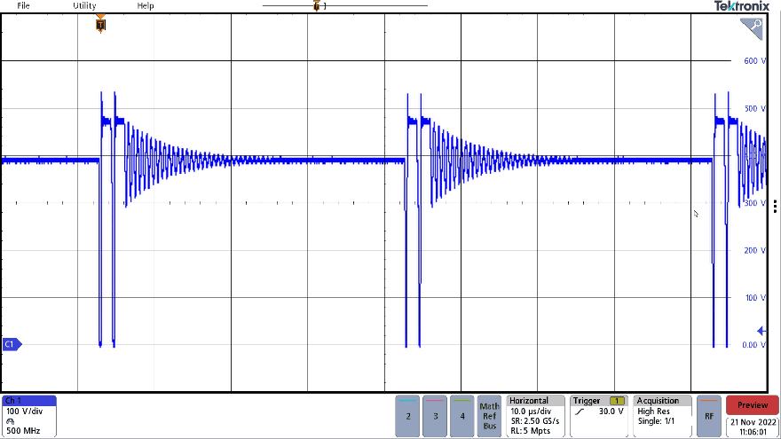 Figure 2-4 Primary Switch Node
Voltage in LPM (250 mA on 12VSB)
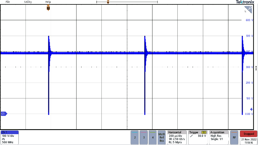 Figure 2-6 Primary Switch Node
Voltage in SBP2 (20 mA on 12VSB)
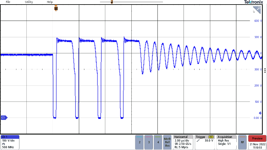 Figure 2-7 Primary Switch Node Voltage in SBP2 (Zoom) (20
mA on 12VSB)