TIDUBY9 December 2021
- Description
- Resources
- Features
- Applications
- 5
- 1System Description
-
2System Overview
- 2.1 Block Diagram
- 2.2 Highlighted Products
- 2.3
Design Considerations
- 2.3.1
Design Hardware Implementation
- 2.3.1.1 Hall-Effect Switches
- 2.3.1.2 Linear Hall-Effect Sensor Output
- 2.3.1.3 Power Supply
- 2.3.1.4 Transistor Circuit for Creating High-Voltage Enable Signal
- 2.3.2 Alternative Implementations
- 2.3.1
Design Hardware Implementation
- 3Hardware, Software, Testing Requirements, and Test Results
- 4Design and Documentation Support
2.3.1.2.3 DRV5056 Placement
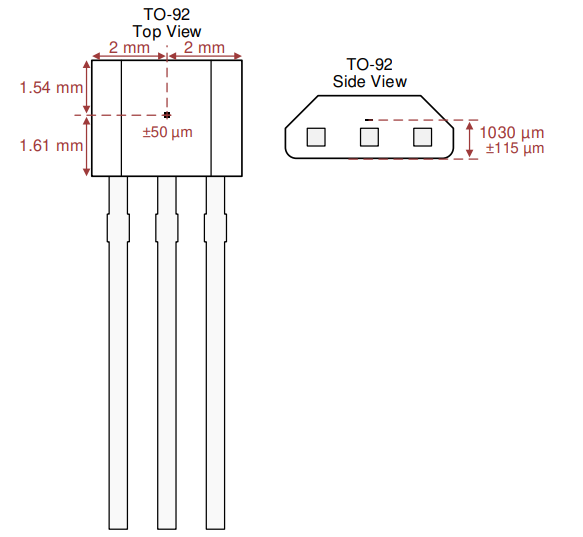
Similar to the DRV5032, the magnetic flux density detected by the DRV5056 is dependent on the magnet dimensions, magnet material, and the distance from the magnet to the sensing element within the Hall sensor. The DRV5056 device in this design uses the TO-92 through-hole package. Figure 2-21 shows the location of the sensing element for this package of the DRV5056. The sensing element is located about 1.03 mm from the back side of the package. If the TO-92 width is 1.62 mm, the distance from the front of the package to the sensing element is 0.61 mm.
 Figure 2-21 Location of Sensing Element Within TO-92 Package of DRV5056
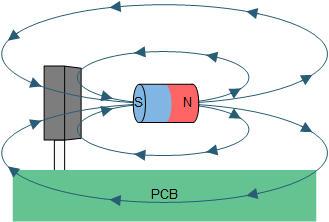
The DRV5056 is a unipolar device that only responds to a positive field. The device detects a positive field when a south magnetic pole is near the front (marked-side) of the package, as shown in Figure 2-22. The device can also detect a positive field when the north pole of a magnet is applied behind the back of the package.
 Figure 2-22 DRV5056 Flux Density Polarity
In this design, the north pole of the magnet is applied behind the back of the package. This made for a slightly more compact design due to the Hall element placement within the package being further from the back of the package than the front of the package. If desired, the polarity and direction of approach could be changed to a south pole from the front. If this is done, then switches U1 and U2 need to swap polarities.
Based on the magnet specifications and the distance from the magnet to the sensing elements, a calculation of the magnetic flux density was done to find a proper placement of the DRV5056 by using the DRV5056 Distance Measurement Tool. This tool is able to calculate magnetic flux density for the head-on configuration used in this design, assuming that there are no x or y displacements from the center of the magnet to the sensing element. For more information, see the Head-on Linear Displacement Sensing Using Hall-Effect Sensors application brief. Since the displacement input is based on the distance from the magnet to the sensing element instead of the magnet to the top of the package, it can calculate the magnetic flux density detected when the magnet is behind the Hall sensor package as well as when the magnet is in front of the Hall sensor package.
The following procedure was used to find the placement of the DRV5056:
- 0 mm is selected for the x-component and y-component displacements from the dot on the magnet in Figure 2-14 to the sensing element.
- The z-component displacement from the dot on the magnet in Figure 2-14 to the sensing element was selected.
- The DRV5056 distance measurement tool and simulations were used to estimate the magnetic flux density detected at the DRV5056 across the entire 10-mm trigger displacement distance. The DRV5056 displacement tool can be used in this case due to the x and y displacements being 0 mm. For both the distance measurement tool and the simulations, the distances from the magnet to the sensing element must be used instead of the distance from the magnet to either the front or back of the package.
- Based on the maximum magnetic flux density estimated, the DRV5056 variant was selected so that the maximum magnetic flux density is around the maximum magnetic flux density that can be sensed by that device variant. If the estimated maximum magnetic flux density is not near the full range of any of the DRV5056 device variants, take the following steps:
- Restart from step 2 with a different z-component displacement. To increase the maximum magnetic flux density by the sensor, use a smaller z displacement. To decrease the maximum magnetic flux density by the sensor, use a larger z displacement.
- Modify the dimensions or material of the magnet and restart from step 2. Note that the impact of this change on the DRV5032 switch U1, U2, U3, and U4 must be verified.
Based on implementing the previous procedures, the following distances were obtained and used for this design:
- X-component displacement= 0 mm
- Y-component displacement = 0 mm
- Z-component displacement
- Trigger not pressed
- Z-component from white dot of magnet to back of DRV5056 package = 6.4 mm
- Z-component from white dot of magnet to sensing element (d1 in tool) = 7.4 mm
- Maximum trigger displacement = 10 mm
- Z-component from white dot of magnet to back of DRV5056 package = 16.4 mm
- Z-component from white dot of magnet to sensing element to sensing element (d2 in tool) = 17.4 mm
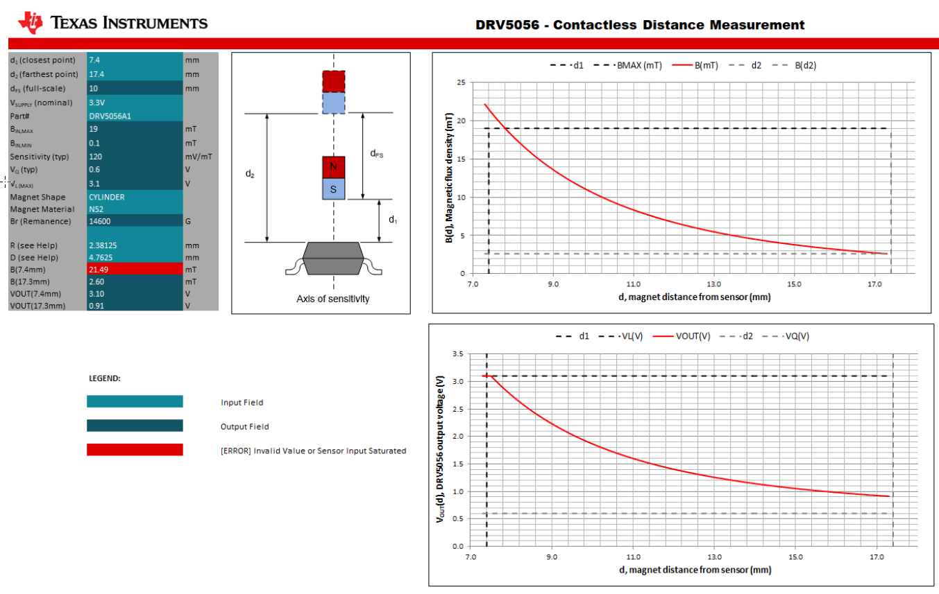
Figure 2-23 shows the settings used to estimate the magnetic flux density for the DRV5056. Once the settings have been entered into the tool, the tool calculates a table of the magnetic flux density. Figure 2-24 is the corresponding magnetic flux density graph, which includes the magnetic flux density waveform obtained from simulation and the magnetic flux density calculated by the DRV5056 distance measurement tool. Similarly, Figure 2-25 shows the simulated and calculated output voltage of the DRV5056.
 Figure 2-23 Distance Measurement Tool Settings for DRV5056Figure 2-24 Simulated and Calculated Magnetic Flux Density at DRV5056
 - Trigger not pressed
- Figure 2-25 Simulated and Calculated DRV5056 Output Voltage