TIDUC99 August   2022 TPSM82903


  1.   Description
  2.   Resources
  3.   Features
  4.   Applications
  5.   5
  6. 1System Description
  7. 2System Overview
    1. 2.1 Block Diagram
    2. 2.2 Design Considerations
    3. 2.3 Highlighted Products
    4. 2.4 System Design Theory
      1. 2.4.1 Buck Converter Circuit Design Using TPSM82903
  8. 3Hardware, Software, Testing Requirements, and Test Results
    1. 3.1 Hardware Requirements
    2. 3.2 Test Setup
    3. 3.3 Test Results
      1. 3.3.1 Startup
      2. 3.3.2 Shutdown
      3. 3.3.3 Load Transient
      4. 3.3.4 Output Ripple
      5. 3.3.5 Efficiency
      6. 3.3.6 Thermal Performance
      7. 3.3.7 Output Voltage vs. Output Current
  9. 4Design and Documentation Support
    1. 4.1 Design Files
      1. 4.1.1 Schematics
      2. 4.1.2 BOM
      3. 4.1.3 PCB Layout Recommendations
        1. 4.1.3.1 Layout Prints
      4. 4.1.4 Altium Project
      5. 4.1.5 Gerber Files
      6. 4.1.6 Assembly Drawings
    2. 4.2 Documentation Support
    3. 4.3 Support Resources
    4. 4.4 Trademarks

Thermal Performance

Thermal performances measured at 2.5-A and 2-A loads. The TPSM82903 is designed for maximum junction temperature of 125°C. These images were captured under room temperature, which is approximately 27°C. The measurements were taken with no air flow present and the thermal camera placed horizontally at a distance of 5-inches from the camera. The peak temperature typically occurs at the center of the board where the inductor and the converter are located.
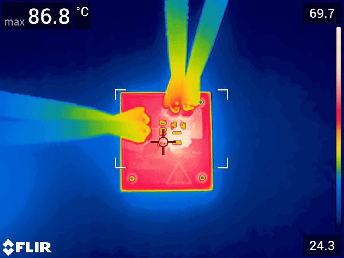
GUID-20220801-SS0I-KB2H-S5NX-PFFQPVW8959C-low.jpgFigure 3-10 Thermal Image at Room Temperature with 12-Vin, 1.2-Vo, 2.5-A
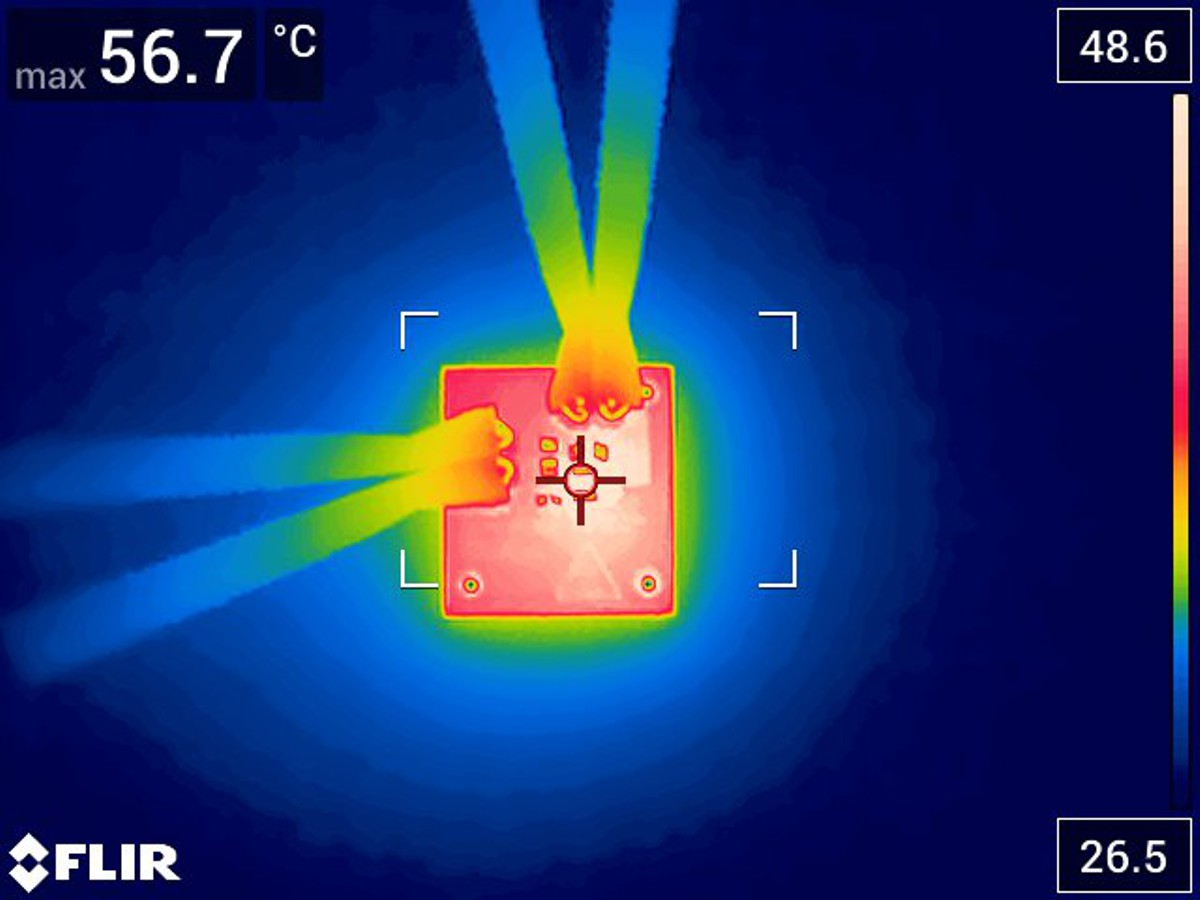
GUID-20220801-SS0I-MGRM-Z6H9-GVBWC5KPQRD0-low.jpgFigure 3-11 Thermal Image at Room Temperature with 12-Vin, 1.2-Vo, 2-A