TIDUCL0 January 2017
- 1 Description
- 2 Resources
- 3 Features
- 4 Applications
- 5 Design Images
- 6 System Overview
-
7 System Design Theory
- 7.1 Power Stage Design—Battery Power Input to the Board
- 7.2 Power Stage Design—Three-Phase Inverter
- 7.3 Power Stage Design—DRV8323 Gate Driver
- 7.4 Power Stage Design—18-V to 3.3-V DC-DC Converter
- 7.5 Power Stage Design —Microcontroller MSP430
- 7.6 Power Stage Design—Hall Sensor Interface
- 7.7 Temperature Sensing
- 7.8 Power Stage Design—External Interface Options and Indications
- 8 Getting Started Hardware and Software
- 9 Testing and Results
- 10Design Files
- 11Software Files
- 12Related Documentation
- 13Terminology
- 14About the Author
9.2.1.4 MOSFET Switching Waveforms
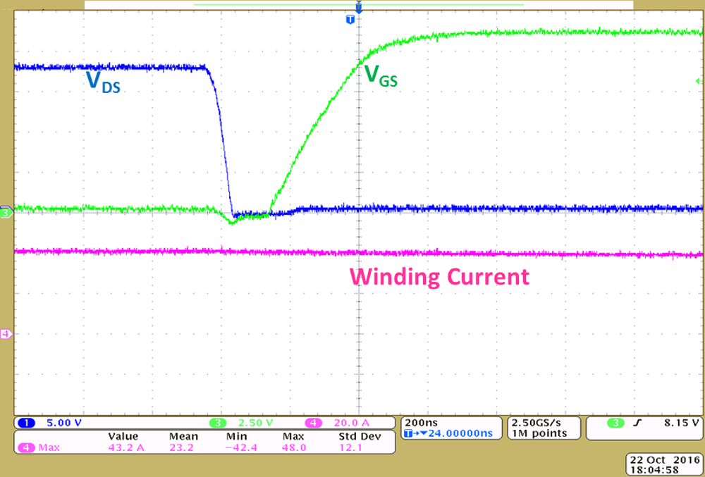
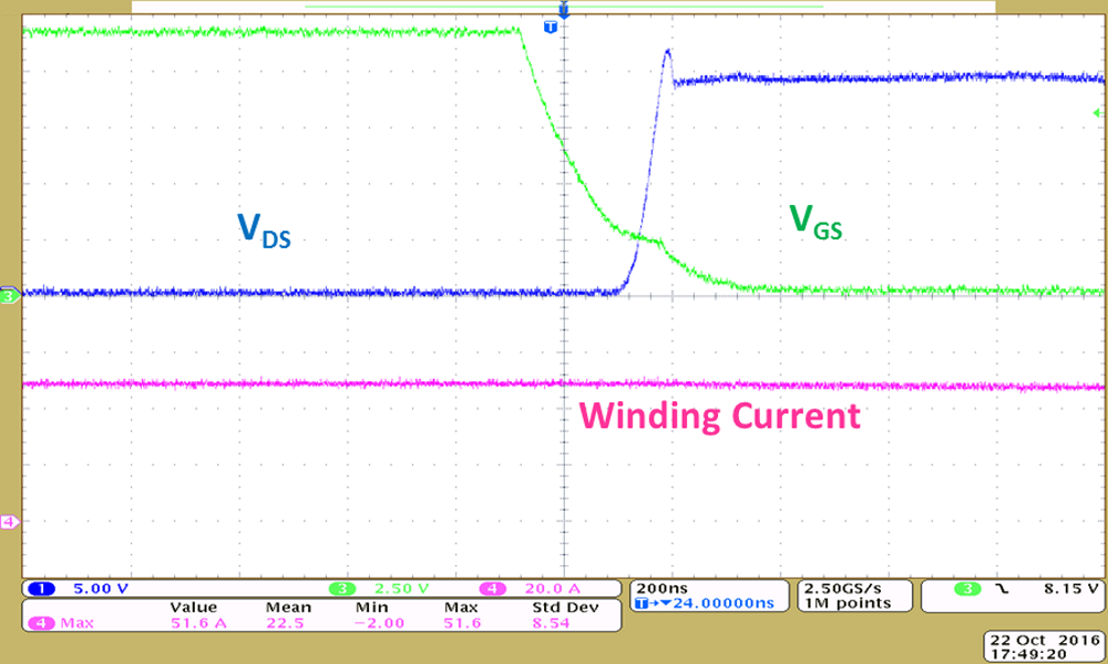
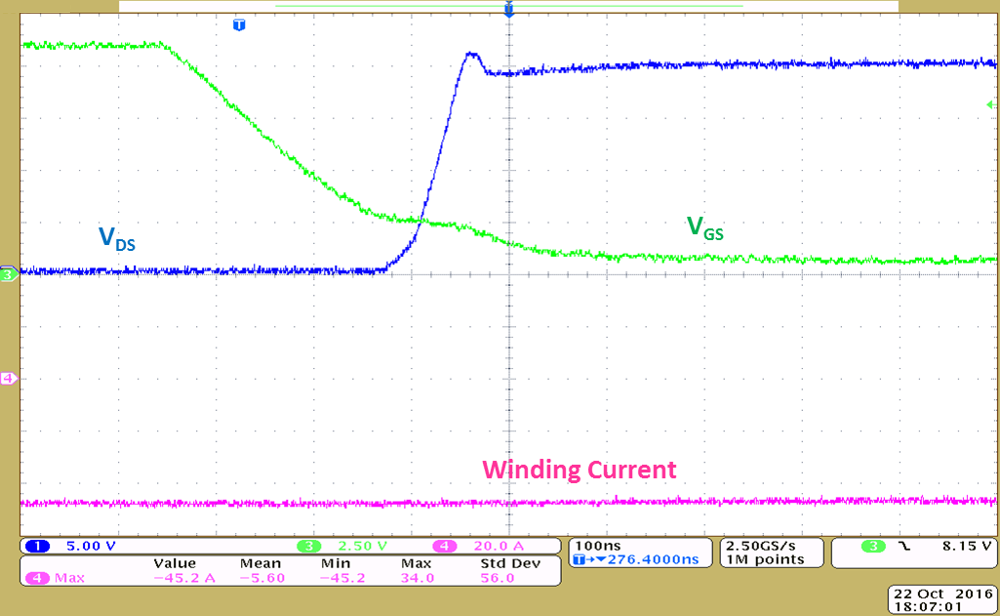
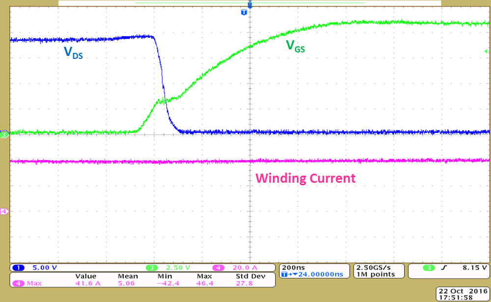
Figure 23 to Figure 26 shows the VDS and VGS waveforms of the low-side and high-side MOSFETs at a total gate current of the DRV8323 (IDRIVE) is set at a 680-mA source and a 2-A sink current. The design uses two FETs in parallel. Therefore, the gate drive current per FET is a 340-mA source and a 1-A sink current. The switching waveforms are captured with a 3.3-Ω gate resistor for each FET. Switching waveforms are clean without any over voltage ringing due to:
- The power block has both the high-side and low-side switches in same package, which reduces the parasitic inductance and hence reduces the phase node voltage ringing.
- The current controlled gate driver with slew rate control helps to optimize the switching.
- The IDRIVE/TDRIVE feature of the gate driver helps to shape the gate current to optimize the switching.
 Figure 23. Turnon—Low-Side VGS and VDS at 43-A Winding Current
  Figure 25. Turnoff—High-Side VGS and VDS at 52-A Winding Current
  Figure 24. Turnoff—Low-Side VGS and VDS at 45-A Winding Current
  Figure 26. Turnon—High-Side VGS and VDS at 42-A Winding Current