TIDUE53I march 2018 – july 2023 TMS320F28P550SJ , TMS320F28P559SJ-Q1
- 1
- Description
- Resources
- Features
- Applications
- 6
- 1System Description
- 2System Overview
-
3Hardware, Software, Testing Requirements, and Test Results
- 3.1 Required Hardware and Software
- 3.2 Testing and Results
- 4Design Files
- 5Trademarks
- 6About the Authors
- 7Revision History
3.2.2.1 Lab 2
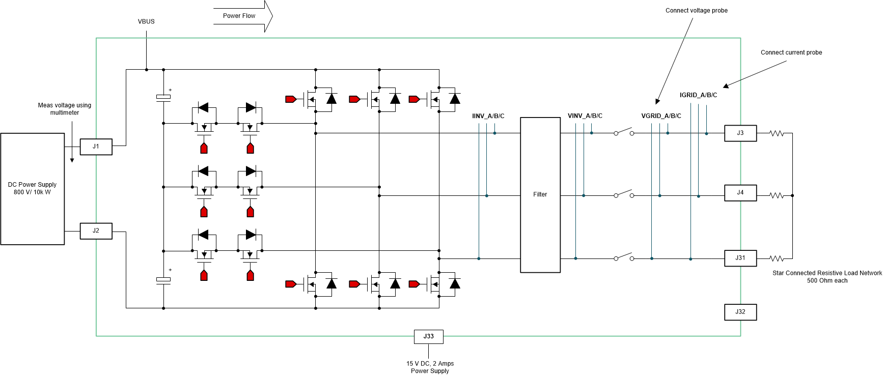
In this lab the power stage is run in an open loop on the HW or HIL platform. Figure 3-5 shows lab setup of the actual hardware.
 Figure 3-5 Inverter Mode With Resistive Load lab Setup
Figure 3-6 shows the SW diagram.
 Figure 3-6 Lab 2 Software Diagram
Refer to the hardware test set up section for actual details of the equipment used for configuring the test. Set the project to Lab 2 by changing the Lab Number in the <settings.h> file, (this will be changed by powerSUITE GUI when using powerSUITE project).
In the user-settings.h file some additional options are available, but the following are used for the tests documented in this user guide.
//
// Option to use SDFM based grid sensing for the current loop
// with this option the inv current from LEM is overwritten by the grid current from SDFM
// On Revision 5 of the hardware the only option supported is the SDFM sensing
//
#define TINV_SDFM 1
#define TINV_ADC 2
#define TINV_CURRENT_LOOP_SENSE_OPTION TINV_SDFM
....
#if TINV_LAB == 2
#define TINV_TEST_SETUP TINV_TEST_SETUP_RES_LOAD
#define TINV_PROTECTION TINV_PROTECTION_ENABLED
#define TINV_SFRA_TYPE TINV_SFRA_CURRENT
#define TINV_SFRA_AMPLITUDE (float32_t)TINV_SFRA_INJECTION_AMPLITUDE_LEVEL2
#define TINV_POWERFLOW_MODE TINV_INVERTER_MODE
#define TINV_DC_CHECK 0
#define TINV_SPLL_TYPE TINV_SPLL_SRF
#endif
Lab 2:
In this check, the SW is run on the hardware, or the HIL platform, or both.
Build and load the code, use the lab2.js file to populate the watch variables in the CCS window.
- Turn on the relay by writing a 1 to TINV_allRelaySet. The auxiliary power supply should draw close to 530 mA.
- Set up an appropriate resistive load around 1 kΩ for the star connected load to start with, although the inverter mode can started at no load as well.
- Slowly ramp the DC bus voltage 'Vbus' to 800 V.
- Set the TINV_clearPWMTrip = 1, to clear the PWM trip signal. Now the switching action begins and sinusoidal voltages start appearing at the output. At this point the auxiliary power supply should draw close to 570 mA.
- TINV_vdInvRef_pu (default value is 0.835) is the modulation index that can be used to vary the AC output of the inverter in open-loop fashion.
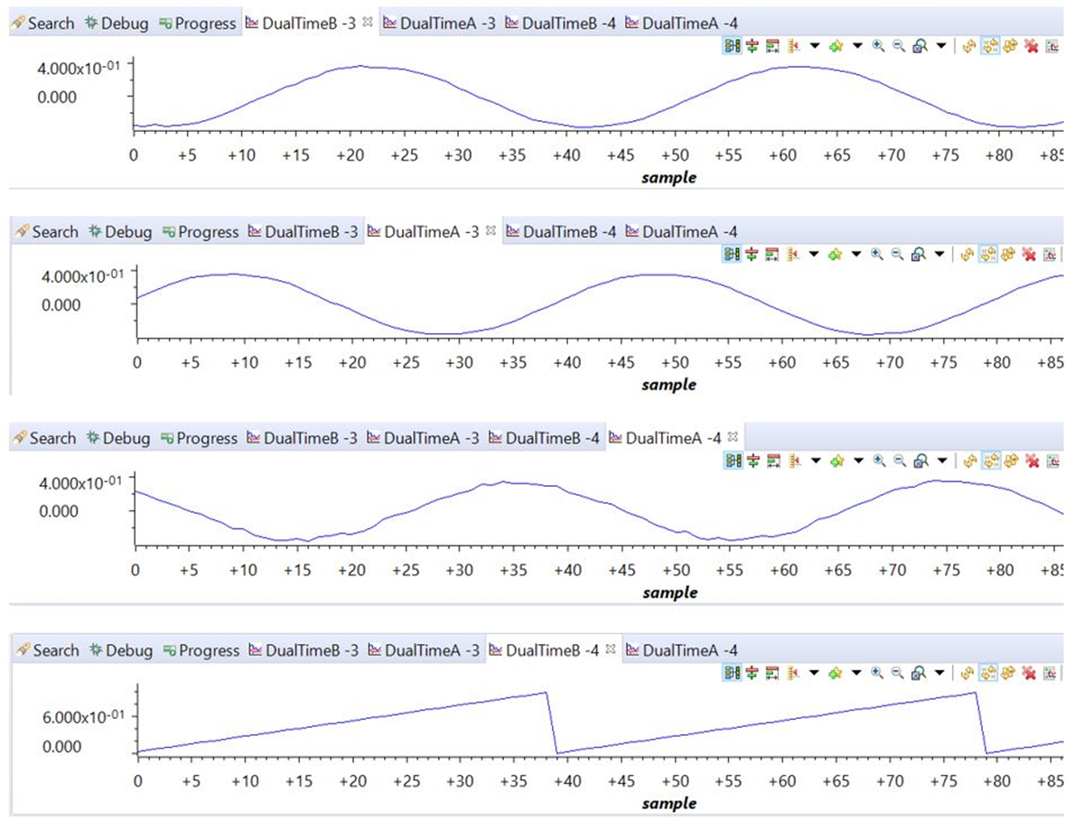
- Verify the sensed voltage and current measurement data in the graph window before proceeding to close the current loop in Lab 3. Figure 3-7 is the graph window for sensed grid side current by using SDFM module of C2000. The scale is shown in per unit (pu).
#ifndef __TMS320C28XX_CLA__
TINV_dVal1 = TINV_iGrid_A_sensed_pu;
TINV_dVal2 = TINV_iGrid_B_sensed_pu;
TINV_dVal3 = TINV_iGrid_C_sensed_pu;
TINV_dVal4 = TINV_rgen.out;
DLOG_4CH_run(&TINV_dLog1);
#endif
Figure 3-7 Sensed Grid Currents
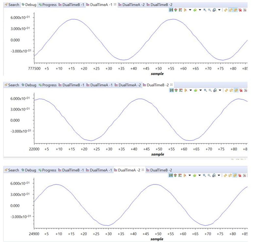
Figure 3-8 shows the three grid voltages monitored from the CCS graph window. The scale is shown in per unit (pu).
 Figure 3-8 Sensed Grid Voltage
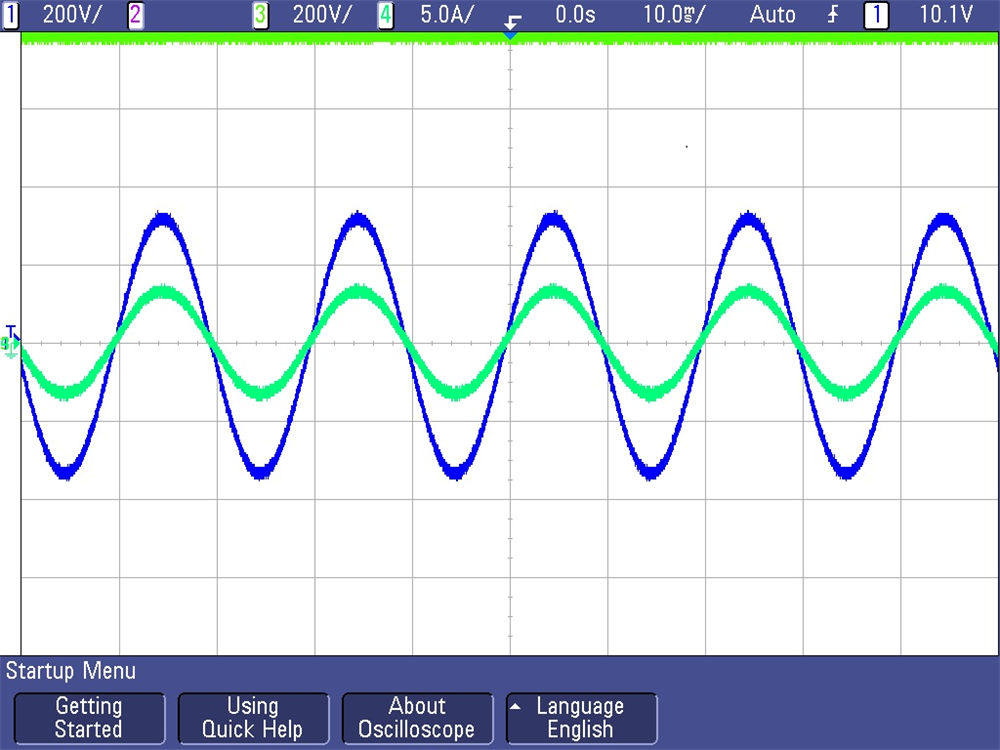
Figure 3-9 shows the captured voltage and current waveform of inverter operating in open loop at 230 VAC and 1.7 kW. Scope signals: Channel 1 - DC link voltage (light green), Channel 2 - AC voltage (blue), Channel 3 - AC current (dark green).
 Figure 3-9 Open Loop Inverter Voltage and Current Waveform