TIDUE53I march 2018 – july 2023 TMS320F28P550SJ , TMS320F28P559SJ-Q1
- 1
- Description
- Resources
- Features
- Applications
- 6
- 1System Description
- 2System Overview
-
3Hardware, Software, Testing Requirements, and Test Results
- 3.1 Required Hardware and Software
- 3.2 Testing and Results
- 4Design Files
- 5Trademarks
- 6About the Authors
- 7Revision History
2.3.6.2 PFC DC Bus Voltage Regulation Loop Design
Before looking at the voltage loop model, the power measurement from DQ domain can be written as:

where 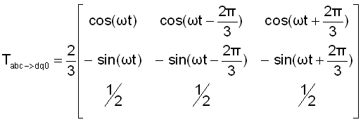
Hence:
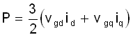
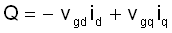
The DC Bus regulation loop is assumed to be providing the power reference, which is divided by the square of the line voltages RMS to provide the conductance. When further multiplied by the line voltage gives the instantaneous current.
 Figure 2-50 Voltage Loop Model
A small-signal model of the DC bus regulation loop is developed by linearizing Equation 52 around the operating point:
Because transformation is an amplitude
invariant, translating from RMS to peak quantities using 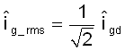 and
and 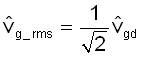 , Equation 53 can be derived.
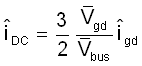
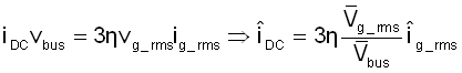
Also for resistive load on the DC Bus:
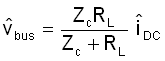 .
.
Therefore, the voltage loop plant can be written as Equation 54
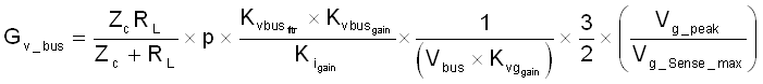
Using the previous model the following compensator, Equation 55 is designed for the voltage loop:
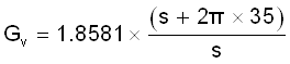
SFRA is used to measure the voltage loop bandwidth, and compare against the model which shows good correlation to the model. Figure 2-51 shows the plant frequency response comparison and Figure 2-52 shows the open-loop frequency response comparison of modelled versus measured.
 Figure 2-51 Voltage Loop Plant Frequency
Response Measured vs Modelled
Figure 2-51 Voltage Loop Plant Frequency
Response Measured vs Modelled Figure 2-52 Voltage Loop, Open-Loop
Frequency Response Modelled vs Measured
Figure 2-52 Voltage Loop, Open-Loop
Frequency Response Modelled vs Measured