TIDUEG2C March 2019 – March 2020
3.1.2.2 Project Structure

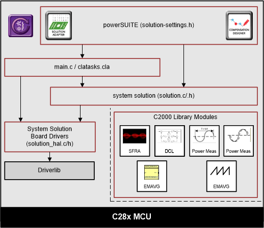
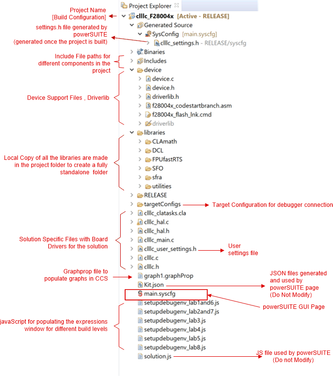
The general structure of the project is shown in Figure 28. Once the project is imported, the Project Explorer will appear inside CCS as shown in Figure 29. Note: Figure 29 shows the project for F28004x; however, if a different device is chosen from the powerSUITE page, the structure will be similar.
Solution-specific and device-independent files that consist of the core algorithmic code are in "<solution>.c/h".
Board-specific and device-specific files are in "<solution>_hal.c/h". This file consists of device-specific drivers to run the solution. If the user wants to use a different modulation scheme or a different device, the user is required only to make changes to these files, besides changing the device support files in the project.
The "<solution>-main.c" file consists of the main framework of the project. This file consists of calls to the board and solution file that help in creating the system framework, along with the interrupt service routines (ISRs) and slow background tasks.
For this design, <solution> is "clllc".
The powerSUITE page can be opened by clicking on the “main.syscfg” file, listed under the Project Explorer. The powerSUITE page generates the "<solution>_settings.h" file. This file is the only C based file used in the compile of the project that is generated by the powerSUITE page. The user must not modify this file manually, as the changes will be overwritten by powerSUITE each time the project is saved. "<solution>_user_settings.h" is included by the "<solution>_settings.h"and can be used to keep any settings that are outside the scope of powerSUITE tools such as #defines for ADC mapping, GPIOs etc.
The “Kit.json” and “solution.js” files are used internally by powerSUITE and also must not be modified by the user. Any changes to these files will result in the project not functioning properly.
The solution name is also used as the module name for all the variables and defines used in the solution. Hence, all variables and function calls are prepended by the CLLLC name (for example, CLLLC_vSecSensed_pu). This naming convention lets the user combine different solutions while avoiding naming conflicts.
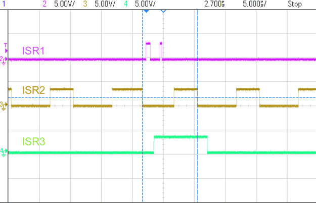
The CLLLC project consists of three ISRs (ISR1, ISR2, and ISR3) with ISR1 being the fastest and non-nestable ISR.
ISR1 is reserved for the PWM update ISR. ISR1 is triggered by the PRIM_LEG1_PWM_BASE → EPWM_INT_TBCTR_U_CMPC event. In general, this interrupt is disabled by writing a value to CMPC, which is greater than all possible TBPRD register values for PRIM_LEG1_PWM_BASE. This is done through the CLLLC_HAL_setupISR1Trigger function. Following are the defines that are related to this ISR.
#define CLLLC_ISR1_PERIPHERAL_TRIG_BASE CLLLC_PRIM_LEG1_PWM_BASE
#define CLLLC_ISR1_TRIG INT_EPWM1
#define CLLLC_ISR1_PIE_GROUP INTERRUPT_ACK_GROUP3
#define CLLLC_ISR1_TRIG_CLA CLA_TRIGGER_EPWM1INT
ISR2 is responsible for writing a valid value to trigger ISR1 by a write to CMPC when ISR1 is desired. (Note: The CMPC is not tied to the global load mechanism to enable this. Also, shadow load of CMPC is disabled.) The CMPC value can be adjusted to get the desired timing from the ISR1. Each time ISR1 is enabled, it triggers two times. In the first ISR1, PWM registers are updated and a sync is enabled. In the second ISR1, the PWM sync is disabled and CMPC is set to a value such that ISR1 does not trigger again. For simplicity the software diagrams and structure only show ISR1 that is triggered the first time.
ISR2 is periodically triggered at ISR2_FREQUENCY. A spare CAP module is used to generate the time base and trigger the interrupt. A spare ePWM module is also configured with the same time base and is used to trigger the ADC conversions. ISR2 is responsible for running the control law and calculating the clock ticks required for the PWM. Once the writes to the shadow registers are complete, the ISR2 enables the ISR1 trigger by writing a valid value (that is, one that is less than the current TBPRD register) to the CMPC register. ISR2 has two variants ISR2_primToSecPowerFlow and ISR2_secToPrimPowerFlow, one for the power flow from primary to secondary side and other for secondary to primary. This is done to to optimize CPU cycles when controlling power flow in different directions. For simplicity of explaination either of them are just referred to as ISR2 in respective labs. Depending on the timing, the ISR1 may nest ISR2 for the update writes, which are very timing-critical. Following are the defines that are related to this ISR.
#define CLLLC_ISR2_ECAP_BASE ECAP1_BASE
#define CLLLC_ISR2_PWM_BASE EPWM5_BASE
#define CLLLC_ISR2_TRIG INT_ECAP1
#define CLLLC_ISR2_PIE_GROUP INTERRUPT_ACK_GROUP4
#define CLLLC_ISR2_TRIG_CLA CLA_TRIGGER_ADCA2
ISR3 is triggered by ADCINT2, which is initiated by a conversion that is started using a CPU timer. It is used to run housekeeping functions such as doing a running average on the currents and voltage signals to remove noise, and running the slew rate function for commanded references.
#define CLLLC_ISR3_TIMEBASE CLLLC_TASKC_CPUTIMER_BASE
#define CLLLC_ISR3_PERIPHERAL_TRIG_BASE ADCC_BASE
#define CLLLC_ISR3_TRIG INT_ADCC2
#define CLLLC_ISR3_PIE_GROUP INTERRUPT_ACK_GROUP10
With this, the interrupts can be nested easily. Figure 30 shows the nesting of the three interrupts occurring. The image is taken for the system in open loop and when a period change is initiated through the watch window, hence only one time ISR1 trigger is observed. For a closed-loop system, the period will only have minor changes from one control ISR cycle to the other and hence the ISR1 will be triggered repeatedly.

Additionally, CPU timers are used to trigger slow background tasks (these are not interrupt-driven but polled).
"A" tasks are triggered at TASKA_FREQ, which is 100 Hz. The SFRA GUI must be called at this rate. One task, A1, is executed at this rate.
"B" tasks are triggered at TASKB_FREQ, which is 10 Hz. These are used for some basic LED toggles and state machine items that are not timing-critical. Three tasks—B1, B2, B3—are serviced by this; hence, each has an execution rate of 3.33 Hz.
#define TASKA_FREQ 100
#define TASKB_FREQ 10
The software of this reference design is organized in eight labs, with incremental builds (INCR_BUILD) and project options (CLLLC_CONTROL_MODE, CLLLC_SEC_CONNECTED_IN_BATTERY_EMULATION_MODE). These tests simplify the system bringup and design.
Lab 1:Primary to Secondary Power Flow, Open Loop Check PWM driver, no high power applied to the board. See Section 3.2.2.1
Lab 2: Primary to Secondary Power Flow, Open Loop Check PWM driver and ADC with protection, resistive load connected on secondary. See Section 3.2.2.2.
Lab 3:Primary to Secondary Power Flow, Closed Voltage Loop Check, with resistive load connected on secondary. See Section 3.2.2.3.
Lab 4: Primary to Secondary Power Flow, Closed Current Loop Check, with resistive load connected on secondary. See Section 3.2.2.4.
Lab 5:Primary to Secondary Power Flow, Closed Current Loop Check, with resistive load connected on secondary in parallel to a voltage source to emulate a battery connection on secondary side. See Section 3.2.2.5.
Lab 6: Secondary to Primary Power Flow, Open Loop Check PWM driver, no high power applied to the board. See Section 3.2.2.6
Lab 7: Secondary to Primary Power Flow, Open Loop Check PWM driver and ADC with protection, resistive load connected on primary. See Section 3.2.2.7
Lab 8: Secondary to Primary Power Flow, Closed Voltage Loop Check, with resistive load connected on primary. See Section 3.2.2.8
These defines are in the "settings.h" file, and can be changed through the powerSUITE settings page.
