TIDUF06 August 2022
- Description
- Resources
- Features
- Applications
- 5
- 1System Description
- 2System Overview
- 3Hardware, Testing Requirements, and Test Results
- 4Design Files
- 5Related Documentation
- 6Trademarks
4.3.3 Serializer Layout Recommendations
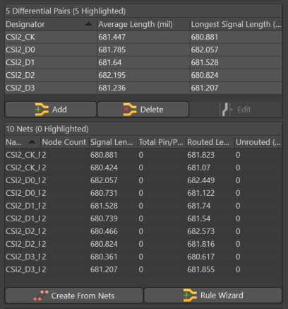
Trace impedance is one critical aspect to the CSI-2 lane routing. For trace impedance to be within specifications and within range of each other, the length and width of the trace plays a factor in this. To achieve tight impedance specs, length specifications also need to be strict within the positive-to-negative differential pair length and pair-to-pair length. If the length is not matched, at these high-data switching speeds, the data can arrive at the 953 at different times and cause issues of synchronization between data and clock. The length difference between the positive and negative differential pair trace should be within 5 mils of each other. For length matching between each CSI-2 lane pair, the difference must be kept within 25 mils.
 Figure 4-4 CSI Routing Matching
The last key points to address with CSI-2 routing is crosstalk and reflections. To reduce the effects of crosstalk between lanes, spacing between each differential lane must be at least three times the signal trace width. In addition, keep vias and bends on the traces to a minimum. Bends must be as equal as possible in the number of left and right bends, and the angle of the bend must be greater than or equal to 135 degrees.
Decoupling capacitors need to be located very close to the supply pin on the serializer. Again, this requires that the user consider the path of the supply current and the return current. Keeping the loop area of this connection small reduces the parasitic inductance associated with the connection of the capacitor. Due to space constraints, ideal placement is not always possible. For decoupling capacitors placed on the opposite layer of the serializer, the return path to the serializer thermal pad should be minimized. Smaller value capacitors that provide higher frequency decoupling must be placed closest to the device.
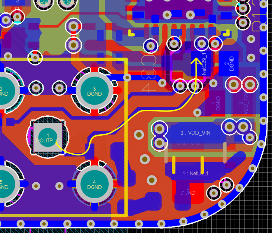
For this application, a single-ended impedance of 50 Ω is required for the coax interconnect. Whenever possible, this connection must also be kept short. Figure 4-5 shows the routing of the high-speed serial line, highlighted by the yellow line. The total length of the yellow line is about ½ inch.
 Figure 4-5 DOUT Path on Base Board