TIDUF22 January 2023
- Description
- Resources
- Features
- Applications
- 5
- 1System Description
-
2System Overview
- 2.1 Block Diagram
- 2.2
Design Considerations
- 2.2.1 6-W Auxiliary Power Supply
- 2.2.2 AC Input Current Sensing
- 2.2.3 DC Bus Voltage Sensing
- 2.2.4 AC Input Voltage Sensing
- 2.2.5 GaN Driving
- 2.2.6 Inrush Current Protection at Powering On
- 2.2.7 Overcurrent Protection
- 2.2.8 AC Input Undervoltage Protection
- 2.2.9 DC Bus Overvoltage Protection
- 2.2.10 GaN Temperature Monitor and Protection
- 2.2.11 Heat Sink Temperature Monitor and Protection
- 2.2.12 UART Heartbeat Report
- 2.2.13 Motor Control Interface
- 2.3 Highlighted Products
- 3Hardware, Software, Testing Requirements, and Test Results
- 4Design and Documentation Support
- 5About the Author
3.1 Hardware Requirements and Assembly
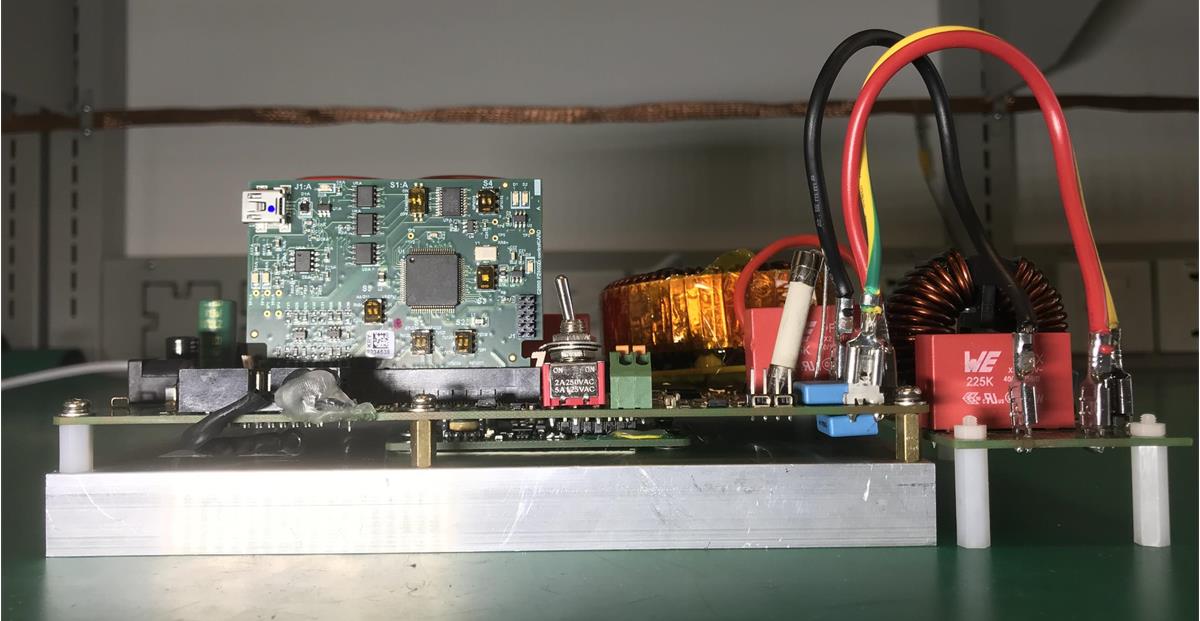
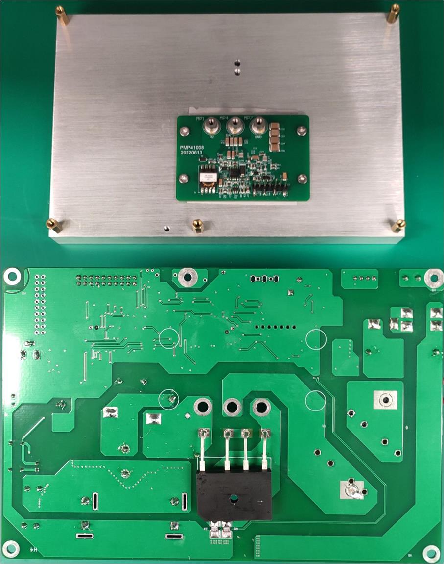
This design has 4 parts: heat sink, GaN daughterboard, main board, and filter board.Figure 3-1 shows the side view of the kit, Figure 3-2 shows relative position of the heat sink, GaN daughterboard, and main board. Two top-side cooled GaN LMG3522R030 devices are adopted on the bottom side of the GaN daughterboard so the devices can be cooled down with the heat sink and diode bridge. The kit is usually shipped fully-assembled; however, the assembly steps are provided in the following list.
- Mount 5-pieces M3 × 10-mm standoffs (3-mm male end with outside thread and female on the other end with inner thread) to heat sink corners.
- Adhere thermal interface materials (TIM), (0.5 mm thickness, Fujipoly GR80A-0H-050GY in this design) on heat sink underneath the GaN daughterboard, make sure TIM is big enough, at least 3 mm extended from any bottom pins and traces of the GaN daughterboard. But 4 pieces of the mechanical holes need 7-mm diameter keepout of TIM.
- Locate the GaN daughterboard on the heat sink with 4 bottom side standoffs aligned to the four mechanical mounting holes on the heat sink. Fasten 4-pcs M3 × 6-mm from the GaN daughterboard to the heat sink.
- Place thermal grease on the bottom side of the diode bridge.
- Fix the heat sink temperature probe to the heat sink with an M3 × 4-mm screw.
- Align J2 of the GaN daughterboard and J4 of main board, J2 can slide into J4 from the bottom side holes of J4.
- Align the main board corner holes to 5-pcs standoffs on the heat sink, and fasten them with M3 × 8-mm screws.
- Align the diode bridge holes to the corresponding holes on the heat sink, and fasten the diode bridge to the heat sink with an M3 × 8-mm screw.
- Screw down 3-pcs M3 × 6-mm screws from the main board holes (HV, SW, and GND) to MP1, MP4, and MP7 standoffs on the GaN daughterboard. These 3-piece screws also act as high-current path between the GaN daughterboard and main board.
- Connect the main board (J1,J2, and J3) to the filter board (J2, J4, and J10) with harness.
- Connect the DC output cable at J5 and J7 on the main board.
- Connect the AC input cable at J1, J3, and J5 on the filter board.
 Figure 3-1 TIDA-010236 Reference Design Side View
 Figure 3-2 Heat Sink, GaN Daughterboard, and Main Board