TIDUF68 February   2024


  1.   1
  2.   Description
  3.   Resources
  4.   Features
  5.   Applications
  6.   6
  7. 1System Description
    1. 1.1 Key System Specifications
  8. 2System Overview
    1. 2.1 Block Diagram
    2. 2.2 Design Considerations
    3. 2.3 Highlighted Products
      1. 2.3.1 LMG2100
      2. 2.3.2 INA241A
      3. 2.3.3 LMR38010
  9. 3System Design Theory
    1. 3.1 Three-Phase GaN Inverter Power Stage
      1. 3.1.1 LMG2100 GaN Half-Bridge Power Stage
    2. 3.2 Inline Shunt Precision-Phase Current Sensing With INA241A
    3. 3.3 Phase Voltage and DC Input Voltage Sensing
    4. 3.4 Power-Stage PCB Temperature Monitor
    5. 3.5 Power Management
      1. 3.5.1 48V to 5V DC/DC Converter
      2. 3.5.2 5V to 3.3V Rail
    6. 3.6 Interface to Host MCU
  10. 4Hardware, Software, Testing Requirements, and Test Results
    1. 4.1 Hardware Requirements
      1. 4.1.1 TIDA-010936 PCB Overview
      2. 4.1.2 TIDA-010936 Jumper Settings
      3. 4.1.3 Interface to C2000™ MCU LaunchPad™ Development Kit
    2. 4.2 Software Requirements
    3. 4.3 Test Setup
    4. 4.4 Test Results
      1. 4.4.1 Power Management and System Power Up and Power Down
    5. 4.5 GaN Inverter Half-Bridge Module Switch Node Voltage
      1. 4.5.1 Switch Node Voltage Transient Response at 48V DC Bus
        1. 4.5.1.1 Output Current at ±1A
        2. 4.5.1.2 Output Current at ±10A
      2. 4.5.2 Impact of PWM Frequency to DC-Bus Voltage Ripple
      3. 4.5.3 Efficiency Measurements
      4. 4.5.4 Thermal Analysis
      5. 4.5.5 No Load Loss Test (COSS Losses)
  11. 5Design and Documentation Support
    1. 5.1 Design Files {Required Topic}
      1. 5.1.1 Schematics
      2. 5.1.2 BOM
      3. 5.1.3 PCB Layout Recommendations
        1. 5.1.3.1 Layout Prints
      4. 5.1.4 Altium Project
      5. 5.1.5 Gerber Files
      6. 5.1.6 Assembly Drawings
    2. 5.2 Tools and Software
    3. 5.3 Documentation Support
    4. 5.4 Support Resources
    5. 5.5 Trademarks
  12. 6About the Author
  13. 7Recognition

48V to 5V DC/DC Converter

The DC/DC buck converter was designed for an input voltage range from 12V to 60V with at least 80V input voltage capability. The output voltage was set to 5V. The DC/DC buck converter feedback circuit was designed for minimum output voltage ripple and at least 1A output current.

The power supply was entirely designed using WEBENCH® circuit design and selection simulation services, using the following parameter specifications:

Table 3-1 Parameter Specifications
PARAMETERTYPICAL VALUEMIN, MAX VALUE
DC-link voltage48V10V, 80V
Output voltage5V±5%
Output voltage ripple< 50mVPPAs low as possible
Output current500mA1A
Temperature range–40°C to 85°C (125°C)

With these parameters the LMR38010 was the device chosen to fit the design specification. Figure 3-7 shows the WEBENCH recommendation.


GUID-20240220-SS0I-L6D6-FZGW-Q2R9K3WF81NZ-low.svg

Figure 3-7 LMR38010 WEBENCH Simulation Circuit

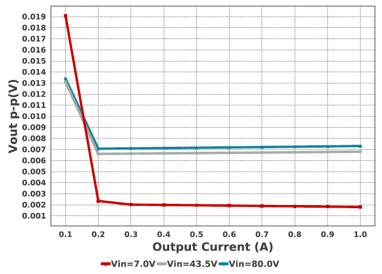
To reduce the size as much as possible, the switching frequency is set to 617kHz (Rt = 42.2kHz), which only requires a 22μH inductor. The voltage ripple is shown in Figure 3-8, for 43.5V input. The output ripple is less than 15mV when the current is >0.1A.

GUID-20240221-SS0I-N3TN-4CZX-RSJZHJCKZ23S-low.png

Figure 3-8 5V Output Voltage Ripple

Based on this simulation, some small changes were made to finish the final schematic of this design. Add an optional resistor R68 parallel to R71 to keep the flexibility for the 5.5V output for LDO to generate a lower ripple 5V. The 5.5V can also be input externally through J7.


GUID-20240220-SS0I-Z9CP-M6WD-VS25NR7ZT8HC-low.svg

Figure 3-9 48V to 5V DC/DC Buck Converter