TIDUF74A April 2024 – April 2024
2.3 Highlighted Products
The TPS1641x is an integrated eFuse with accurate power limit or current limit. The device integrates an NFET with RON of 152mΩ. TPS16410, TPS16411, TPS16414 and TPS16415 provide power limiting whereas the TPS16412, TPS16413, TPS16416 and TPS16417 provide current limiting. The TPS16410, TPS16411, TPS16414 and TPS16415 can provide 15-W accurate power limiting for low power circuit (LPCs) as per IEC60335 and UL60730 standards. TPS16410, TPS16411, TPS16412 and TPS16413 also provide IN to OUT short detection and indication on FLT output. IN to OUT short detection eliminates the need of additional eFuse or power limiting circuit in case of IN to OUT short test for IEC60335, UL60730, and similar standards. FLT can be used as input for MCU or FLT can be used to drive an external PFET. TPS1641x devices also provide protection from adjacent pin short and pin short to GND faults. The TPS1641x device also provide configurable blanking time (IDLY or PDLY) and overcurrent protection (IOCP) for transient loads. Load such as motors need higher current for start-up. Blanking time is useful for providing higher current for start-up of loads such as motors. TPS1641x devices have overvoltage protection (OVP), overtemperature protection, and adjustable output slew rate control (dvdt). Vcc and FLT are rated up to 60V and can provide protection up to 60V with an external PFET.
 Figure 2-17 TPS16410
The LMR38020 converter is an easy-to-use synchronous step-down DC/DC converter that operates from a 4.2V to 80V supply voltage. The device is capable of delivering up to 2ADC load current in a small design size. The LMR38020 employs peak-current mode control. The device enters PFM mode at light load to achieve high efficiency for PFM version. A FPWM version is provided to achieve low output voltage ripple, tight output voltage regulation, and constant switching frequency at light load. The device is internally compensated, which reduces design time, and requires few external components. Additional features, such as precision enable and internal soft start, provide a flexible and easy-to-use design for a wide range of applications. Protection features include thermal shutdown, VIN undervoltage lockout, cycle-by-cycle current limit, and hiccup mode short-circuit protection. The family requires few external components and has a pinout designed for a simple PCB layout.
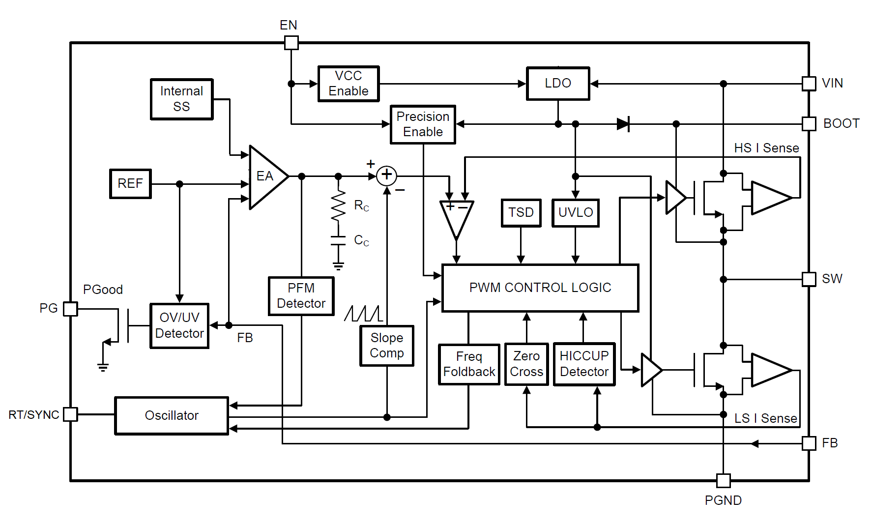 Figure 2-18 LMR38020
The TPS62932 and TPS62933x are 30V, 2A and 3A, synchronous buck (step-down) converters with two integrated n-channel MOSFETs. The TPS62932 and TPS62933x employ fixed-frequency peak current control mode for fast transient response and good line and load regulation. With the optimized internal loop compensation, the devices eliminate the external compensation components over a wide range of output voltage and switching frequency. The integrated 76mΩ and 32mΩ MOSFETs allow for high-efficiency power supply designs with continuous output currents up to 2A (TPS62932) or 3A (TPS62933 and TPS62933x). The feedback reference voltage is designed at 0.8V. The output voltage can be stepped down from 0.8V to 22V. The devices are design for systems powered from 5V, 12V, 19V, and 24V power-bus rails. The TPS6293x has been designed for safe monotonic start-up into prebiased loads. The default start-up is at VIN equal to 3.8V. After the device is enabled, the output rises smoothly from 0V to the regulated voltage. The TPS6293x has low operating current when not switching under no load, especially the TPS62932, TPS62933, and TPS62933P whose operating current is 12μA (typical). When the TPS6293x is disabled, the supply current is approximately 2µA (typical). These features are extremely beneficial for long battery life time in low-power operation.
 Figure 2-19 TPS62932
The DRV8316C device is an integrated 95mΩ (high-side + low-side MOSFETs on-state resistance) driver for 3-phase motor-drive applications. The device reduces system component count, cost, and complexity by integrating three half-bridge MOSFETs, gate drivers, charge pump, current sense amplifiers, linear regulator and buck regulator for external loads. A standard serial peripheral interface (SPI) provides a simple method for configuring the various device settings and reading fault diagnostic information through an external microcontroller. Alternatively, a hardware interface (pin) variant allows for configuring the most commonly used settings through fixed external resistors. The architecture uses an internal state machine to protect against short-circuit events and dv/dt parasitic turn-on of the internal power MOSFETs. The DRV8316C device integrates three, bidirectional current-sense amplifiers for monitoring the current level through each of the half-bridges using a built-in current sense. The gain setting of the amplifier can be adjusted through the SPI or hardware interface. In addition to the high level of device integration, DRV8316C provides a wide range of integrated protection features. These features include power-supply undervoltage lockout (UVLO), charge-pump undervoltage lockout (CPUV), overcurrent protection (OCP), AVDD undervoltage lockout (AVDD_UV), buck regulator UVLO and overtemperature warning and shutdown (OTW and OTSD). Fault events are indicated by the nFAULT pin with detailed information available in the SPI registers on the SPI variant.
 Figure 2-20 DRV8316C
The DRV8428 device is an integrated motor-driver design for bipolar stepper motors. The device provides the maximum integration by integrating two N-channel power MOSFET H-bridges, current sense resistors and regulation circuitry, and a microstepping indexer. The DRV8428 is capable of supporting wide supply voltage range of 4.2V to 33V. DRV8428 provides an output current up to 1.7A peak, 1A full-scale, or 0.7A root mean square (rms). The actual full-scale and rms current depends on the ambient temperature, supply voltage, and PCB thermal capability. The DRV8428 uses an integrated current-sense architecture which eliminates the need for two external power sense resistors, hence saving significant board space, BOM cost, design efforts and reduces significant power consumption. This architecture removes the power dissipated in the sense resistors by using a current mirror approach and using the internal power MOSFETs for current sensing. The current regulation set point is adjusted by the voltage at the VREF pin. A simple STEP/DIR interface allows for an external controller to manage the direction and step rate of the stepper motor. The internal microstepping indexer can execute high-accuracy micro-stepping without requiring the external controller to manage the winding current level. The indexer is capable of full step, half step, and 1/4, 1/8, 1/16, 1/32, 1/64, 1/128, and 1/256 microstepping. High microstepping contributes to significant audible noise reduction and smooth motion. In addition to a standard half stepping mode, a noncircular half stepping mode is available for increased torque output at higher motor RPM. Stepper motor drivers need to re-circulate the winding current by implementing several types of decay modes. The DRV8428 comes with smart tune decay modes. The smart tune is a remarkable decay mechanism that automatically adjusts for the best current regulation performance agnostic of voltage, motor speed, variation and aging effects. Smart tune Ripple Control uses a variable off-time, ripple current control scheme to minimize distortion of the motor winding current. Smart tune Dynamic Decay uses a fixed off-time, dynamic fast decay percentage scheme to minimize distortion of the motor winding current while minimizing frequency content and significantly reducing design efforts. Along with this seamless, effortless automatic smart tune, DRV8428 also provides the traditional mixed decay mode. A low-power sleep mode is included which allows the system to save power when not actively driving the motor.
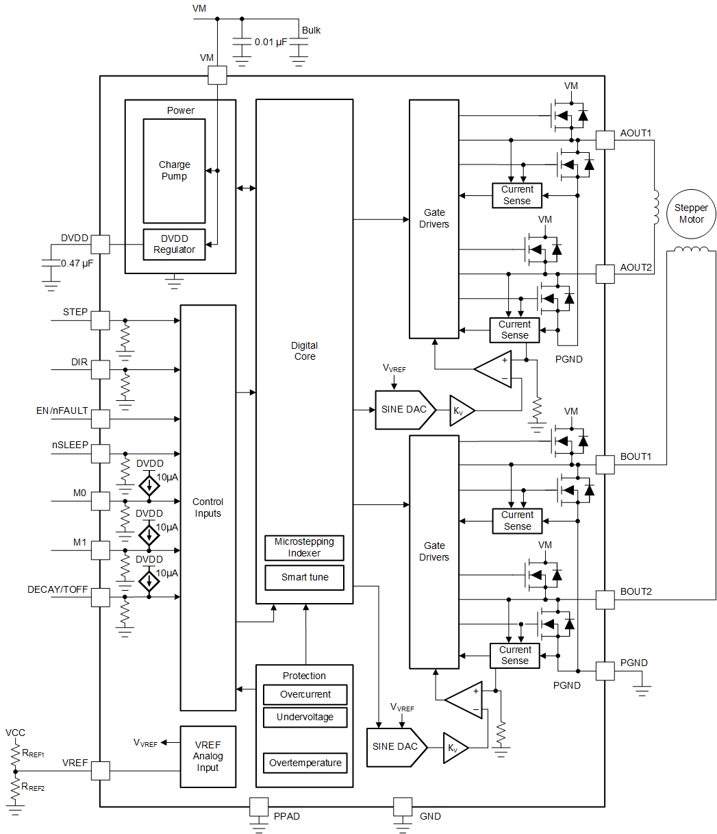 Figure 2-21 DRV8428
The ISO1211 and ISO1212 devices are fully-integrated, isolated digital-input receivers with IEC 61131-2 Type 1, 2, and 3 characteristics. The devices receive 24V to 60V digital-input signals and provide isolated digital outputs. No field-side power supply is required. An external resistor, RSENSE, on the input-signal path precisely sets the limit for the current drawn from the field input based on an internal feedback loop. The voltage transition thresholds are compliant with Type 1, 2, and 3 and can be increased further using an external resistor, RTHR. For more information on selecting the RSENSE and RTHR resistor values, see the Detailed Design Procedure section. The ISO121x devices use an ON-OFF keying (OOK) modulation scheme to transmit the digital data across a silicon-dioxide based isolation barrier. The transmitter sends a high frequency carrier across the barrier to represent one digital state and sends no signal to represent the other digital state. The receiver demodulates the signal after advanced signal conditioning and produces the output through a buffer stage. The conceptual block diagram of the ISO121x device is shown in the Functional Block Diagram section.
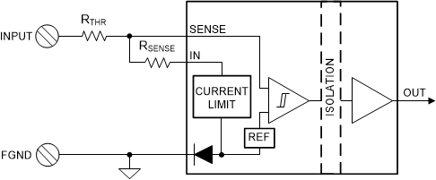 Figure 2-22 ISO1212
This family of CAN transceivers is compatible with the ISO11898-2 High-Speed CAN (controller area network) physical layer standard. The CAN transceivers are designed to interface between the differential bus lines in CAN and the CAN protocol controller.
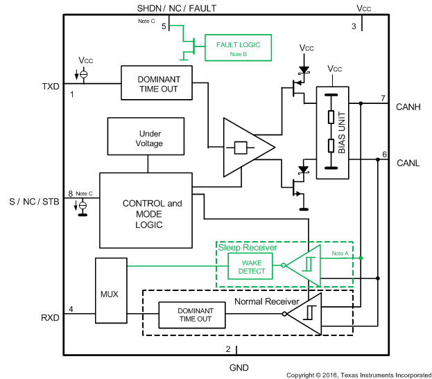 Figure 2-23 TCAN334
MSPM0G350x microcontrollers (MCUs) are part of the MSP highly integrated, ultra-low-power 32-bit MCU family based on the enhanced Arm® Cortex®-M0+ 32-bit core platform operating at up to 80MHz frequency. These cost-optimized MCUs offer high-performance analog peripheral integration, support extended temperature ranges from -40°C to 125°C, and operate with supply voltages ranging from 1.62V to 3.6V. The MSPM0G350x devices provide up to 128KB embedded flash program memory with built-in error correction code (ECC) and up to 32KB SRAM with hardware parity option. These MCUs also incorporate a memory protection unit, 7-channel DMA, math accelerator, and a variety of high-performance analog peripherals such as two 12-bit 4Msps ADCs, configurable internal shared voltage reference, one 12-bit 1Msps DAC, three high speed comparators with built-in reference DACs, two zero-drift zero-crossover op-amps with programmable gain, and one general-purpose amplifier. These devices also offer intelligent digital peripherals such as two 16-bit advanced control timers, five general-purpose timers (with one 16-bit general-purpose timer for QEI interface, two 16-bit general-purpose timers for STANDBY mode, and one 32-bit general-purpose timer), two windowed-watchdog timers, and one RTC with alarm and calendar modes. These devices provide data integrity and encryption peripherals (AES, CRC, TRNG) and enhanced communication interfaces (four UART, two I2C, two SPI, CAN 2.0/FD).
 Figure 2-24 MSPM0G3507
The TMAG5273 IC is based on the Hall-effect technology and precision mixed signal circuitry from Texas Instruments. The output signals (raw X, Y, Z magnetic data and temperature data) are accessible through the I2C interface. The IC consists of the following functional and building blocks:
- The Power Management and Oscillator block contains a low-power oscillator, biasing circuitry, undervoltage detection circuitry, and a fast oscillator.
- The sensing and temperature measurement block contains the Hall biasing, Hall sensors with multiplexers, noise filters, integrator circuit, temperature sensor, and the ADC. The Hall-effect sensor data and temperature data are multiplexed through the same ADC.
- The Interface block contains the I2C control circuitry, ESD protection circuits, and all the I/O circuits. The TMAG5273 supports multiple I2C read frames along with integrated cyclic redundancy check (CRC).
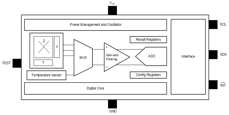 Figure 2-25 TMAG5273
The TLV900x is a family of low-power, rail-to-rail input and output op amps. These devices operate from 1.8V to 5.5V, are unity-gain stable, and are designed for a wide range of general-purpose applications. The input common-mode voltage range includes both rails and allows the TLV900x family to be used in virtually any single-supply application. Rail-to-rail input and output swing significantly increases dynamic range, especially in low-supply applications, and makes them an excellent choice for driving sampling analog-to-digital converters (ADCs).
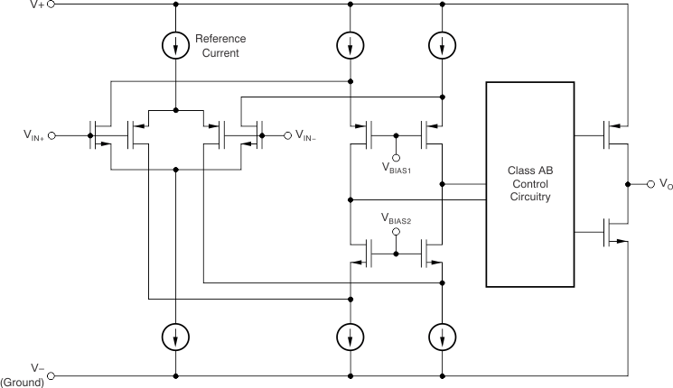 Figure 2-26 TLV9002