TIDUF74A April 2024 – April 2024
3.3 Test Results
TPS16410 E-Fuse Test Results
To test the features of the TPS16410 e-fuse, an electronic load is used to draw the power from the supply. J17 in Figure 3-4 below shows the connection point for the E-load. The input power used for this test is a DC power supply operating at various voltages to capture the controlled start-up, the overvoltage and undervoltage protection response, in addition to the overcurrent protection and power limiting.
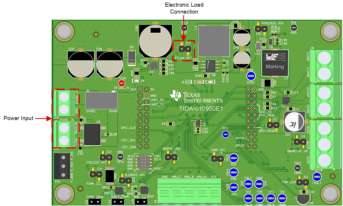 Figure 3-4 Board Connections Used to Test
the TPS16410 E-Fuse
Figure 3-4 Board Connections Used to Test
the TPS16410 E-FuseEFUSE startup, no load
Figure 3-5 below shows the start-up behavior of the TPS16410 when a voltage is applied to the input of the device and incrementally increased to just above the undervoltage threshold. Once the voltage reaches this point, the output voltage of the TPS16410 is enabled and there is a 1.98ms delay from the time the device is enabled to the time the input voltage is available on the output for downstream device power.
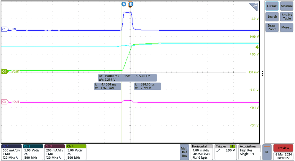 Figure 3-5 E-Fuse Start-up at No Load
Figure 3-6 below shows the response of the TPS16410 when power is turned on with a high load active. In this instance, the TPS16410 starts to regulate the power as expected but due to the inrush current associated with the already active load, the e-fuse eventually goes into a fault condition after approximately 200ms from the time the input voltage is turned on. The input power is limited to 14.30W for this test, yielding an error of approximately 3%.
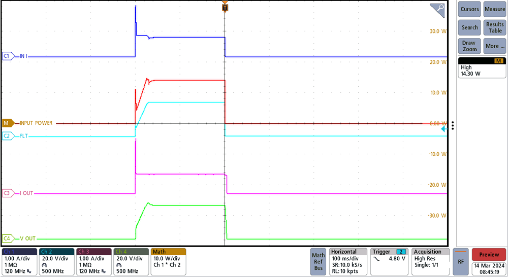 Figure 3-6 E-Fuse Regulation During Voltage Turn-On at High Load
Power Limiting
The TPS16410 circuit is designed to limit the power consumption to 13.65W for this design. For applications requiring a higher power limit (24VAC input), the equations in Section 2.2 can be used to adjust the power limit, or the device can be bypassed for evaluation.
If the device junction temperature reaches the thermal shutdown threshold (TSD), the internal FET is turned off. When the TPS16410 detects thermal overload, the device remains off until cooled down to TSDHYS. Once the TPS16410 has cooled down by TSDHYS, the device remains off for an additional delay of tTSD,RST after which the device automatically retries to turn on if the device is still enabled. During thermal shutdown, the fault pin FLT pulls low to signal a fault condition.
Figure 3-7 below shows the power regulation of the device approaching the 13.7W threshold. The electronic load is set to constant power and gradually increased towards the power limit. As the load increases, the output voltage begins to droop to keep the power below the limit threshold. As the load is increased even more, the device disables the output. The TPS16410 has a power regulation accuracy of 99.5% for a PLIM of 13.65W.
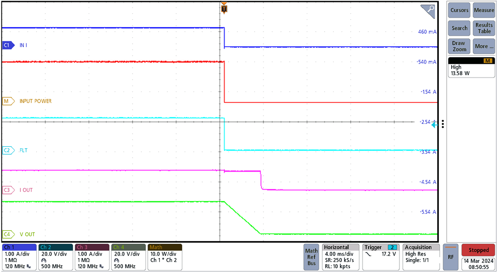 Figure 3-7 E-Fuse Power Limiting
Input Overvoltage protection
The TPS16410 device incorporates circuits to protect the system during overvoltage conditions. A voltage more than the VOVLO threshold on the OVLO pin turns off the internal FET and protects the downstream load. The reference design is designed with overvoltage protection voltage of 28V with an input voltage of 24VDC and approximately 40V for a 24VAC input voltage. Figure 3-8 shows the overvoltage shut down at 28.13V, yielding an OVP accuracy of 99.5% for a 28V OVP threshold.
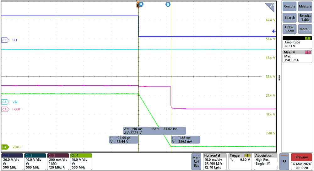 Figure 3-8 E-Fuse Input Overvoltage Protection Response
LMR38020 15V Power Rail Test Results
To test the efficiency of the LMR38020 across loads of 100mA to 1A, both 24VAC as well as 24VDC is provided to J18 and J19, respectively. An electronic load is used to create the specific load conditions for each test. The input voltage, the output voltage, and the output current ripple measurements are taken at the expected maximum allowable load while staying under the 15W total power limit.
Figure 3-9 below shows the voltage ripple of both input and output voltages in addition to the output current ripple for a 1A load on the LMR38020. At this load, the total consumption is right under the limit set by the E-fuse. The input voltage ripple at 1A load is approximately 592mV pk-pk, while the output voltage ripple is approximately 186mV pk-pk. The output current to the load shows a current ripple of approximately 9.3mA, or about 9.3% ripple pk-pk.
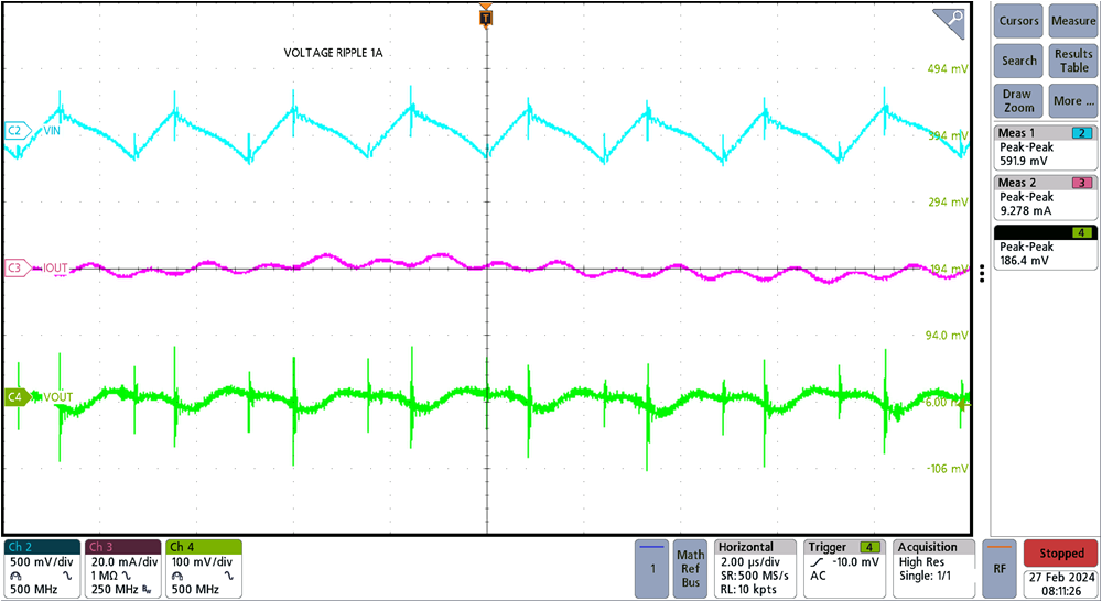 Figure 3-9 LMR38020 Output Voltage Ripple at 1A Load
Efficiency over load test results:
Table 3-1 below shows the test data for a 24VDC input to the LMR38020 with an electronic load on the output to the device. The load current range is increased from 100mA to 1A in 50mA steps.
| VIN (V) | IIN (mA) | VOUT (V) | IOUT (mA) | PIN (W) | POUT (W) | Efficiency | |
|---|---|---|---|---|---|---|---|
| 24 | 66.31 | 15.24 | 97.45 | 1.59 | 1.49 | 93.32 | |
| 24 | 99.94 | 15.23 | 147.00 | 2.40 | 2.24 | 93.34 | |
| 24 | 133.00 | 15.21 | 197.60 | 3.19 | 3.01 | 94.16 | |
| 24 | 164.60 | 15.07 | 247.20 | 3.95 | 3.73 | 94.30 | |
| 24 | 197.04 | 15.07 | 297.03 | 4.73 | 4.48 | 94.66 | |
| 24 | 229.04 | 15.07 | 347.47 | 5.50 | 5.24 | 95.26 | |
| 24 | 261.06 | 15.07 | 397.03 | 6.27 | 5.98 | 95.50 | |
| 24 | 293.92 | 15.07 | 447.16 | 7.05 | 6.74 | 95.53 | |
| 24 | 328.67 | 15.07 | 497.12 | 7.89 | 7.49 | 94.96 | |
| 24 | 361.79 | 15.07 | 547.46 | 8.68 | 8.25 | 95.02 | |
| 24 | 394.57 | 15.07 | 597.16 | 9.47 | 9.00 | 95.03 | |
| 24 | 427.66 | 15.07 | 647.28 | 10.26 | 9.75 | 95.04 | |
| 24 | 461.07 | 15.07 | 697.51 | 11.07 | 10.51 | 94.99 | |
| 24 | 494.42 | 15.07 | 747.47 | 11.87 | 11.26 | 94.93 | |
| 24 | 527.97 | 15.07 | 797.53 | 12.67 | 12.02 | 94.85 | |
| 24 | 561.28 | 15.07 | 846.98 | 13.47 | 12.76 | 94.75 | |
| 24 | 595.32 | 15.06 | 897.36 | 14.29 | 13.51 | 94.59 | |
| 24 | 629.45 | 15.06 | 947.59 | 15.11 | 14.27 | 94.47 | |
| 24 | 663.55 | 15.06 | 997.71 | 15.93 | 15.03 | 94.35 | |
Figure 3-10 below shows the efficiency over load current. The efficiency across all load values is greater than 90%, peaking at 96% efficiency at a 450mA load current.
 Figure 3-10 LMR38020 Efficiency Over Load With 24VDC
Input
Figure 3-10 LMR38020 Efficiency Over Load With 24VDC
InputThe same test is done for a 24VAC rectified input to the LMR38020, sweeping the load current again from 100mA to 1A in 50mA step sizes. This data is captured in Table 3-2 below.
| VIN (V) | IIN (mA) | VOUT (V) | IOUT (mA) | PIN (W) | POUT (W) | Efficiency | |
|---|---|---|---|---|---|---|---|
| 34.53 | 47.93 | 15.23 | 98 | 1.66 | 1.49 | 90% | |
| 34.22 | 72.91 | 15.22 | 147 | 2.49 | 2.24 | 90% | |
| 33.98 | 99.07 | 15.19 | 198 | 3.37 | 3.01 | 89% | |
| 33.78 | 120.37 | 15.06 | 248 | 4.07 | 3.73 | 92% | |
| 33.60 | 144.48 | 15.05 | 297 | 4.85 | 4.47 | 92% | |
| 33.39 | 168.70 | 15.04 | 348 | 5.63 | 5.23 | 93% | |
| 33.22 | 192.62 | 15.04 | 397 | 6.40 | 5.97 | 93% | |
| 33.01 | 218.14 | 15.03 | 447 | 7.20 | 6.72 | 93% | |
| 32.82 | 244.57 | 15.03 | 497 | 8.03 | 7.47 | 93% | |
| 32.61 | 270.47 | 15.03 | 548 | 8.82 | 8.24 | 93% | |
| 32.44 | 296.54 | 15.02 | 597 | 9.62 | 8.97 | 93% | |
| 32.23 | 323.26 | 15.02 | 648 | 10.42 | 9.73 | 93% | |
| 32.03 | 350.78 | 15.02 | 698 | 11.24 | 10.48 | 93% | |
| 31.82 | 378.61 | 15.01 | 748 | 12.05 | 11.23 | 93% | |
| 31.63 | 407.28 | 15.01 | 798 | 12.88 | 11.98 | 93% | |
| 31.42 | 435.92 | 15.00 | 847 | 13.70 | 12.71 | 93% | |
| 31.22 | 465.80 | 15.00 | 898 | 14.54 | 13.47 | 93% | |
| 31.00 | 496.66 | 15.00 | 948 | 15.40 | 14.22 | 92% | |
| 30.78 | 528.17 | 14.99 | 997 | 16.26 | 14.95 | 92% | |
Figure 3-11 below shows the efficiency versus load current for a rectified 24VAC input voltage to the LMR38020. The efficiency peaks at 93% and has a relatively flat efficiency curve from 350mA to 900mA load current.
 Figure 3-11 LMR38020 Efficiency Over Load With 24VAC Input
TPS62932 3.3V Power Rail Test Results
The test procedure for testing the efficiency of the TPS62932 under varying load conditions is identical to the test for the LMR38020 above. In this case, we are pulling 100mA to 1A from the 3.3VDC power rail while providing 15VDC to the input of the buck. This is done to isolate the performance of the 3.3VDC buck.
For the load on the 3.3V power rail, a worst-case scenario of 750mA is used as the load current to measure the input voltage ripple, output voltage ripple, and the output current ripple. Figure 3-12 below shows the ripple for each of the aforementioned parameters. The input voltage ripple pk-pk is 192mV, or approximately 1.3%. The output voltage ripple pk-pk is about 80.8mV, or about 2.4%. The output current ripple pk-pk is around 5.3mA or approximately 0.7%.
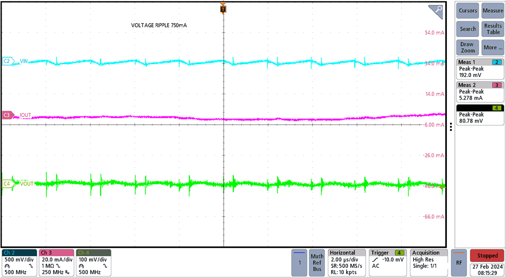 Figure 3-12 TPS62932 Ripple at 750mA Load
Efficiency Results:
Table 3-3 below shows the data captured for the efficiency test of the TPS62932. This test is identical to that of the LMR38020 for load current test values, although the 3.3V power rail total power consumption is much lower since the power rail is only used for the MCU and the board peripherals.
| VIN (V) | IIN (mA) | VOUT (V) | IOUT (mA) | PIN (W) | POUT (W) | Efficiency | |
|---|---|---|---|---|---|---|---|
| 15 | 25.56 | 3.28 | 97.75 | 0.38 | 0.32 | 83.63 | |
| 15 | 39.02 | 3.27 | 147.26 | 0.59 | 0.48 | 82.27 | |
| 15 | 51.06 | 3.27 | 197.82 | 0.77 | 0.65 | 84.46 | |
| 15 | 62.96 | 3.27 | 247.44 | 0.94 | 0.81 | 85.68 | |
| 15 | 74.90 | 3.2 | 297.26 | 1.12 | 0.97 | 86.52 | |
| 15 | 86.85 | 3.27 | 347.68 | 1.30 | 1.14 | 87.27 | |
| 15 | 98.91 | 3.27 | 397.25 | 1.48 | 1.30 | 87.55 | |
| 15 | 110.56 | 3.26 | 447.34 | 1.66 | 1.46 | 87.94 | |
| 15 | 120.11 | 3.26 | 497.31 | 1.80 | 1.62 | 89.99 | |
| 15 | 131.23 | 3.26 | 547.69 | 1.97 | 1.79 | 90.70 | |
| 15 | 142.08 | 3.26 | 597.36 | 2.13 | 1.95 | 91.38 | |
| 15 | 152.94 | 3.26 | 647.48 | 2.29 | 2.11 | 92.01 | |
| 15 | 164.29 | 3.26 | 697.71 | 2.46 | 2.27 | 92.30 | |
| 15 | 175.78 | 3.26 | 747.67 | 2.64 | 2.44 | 92.44 | |
| 15 | 187.34 | 3.26 | 797.72 | 2.81 | 2.60 | 92.54 | |
| 15 | 198.81 | 3.26 | 847.20 | 2.98 | 2.76 | 92.61 | |
| 15 | 210.50 | 3.25 | 897.58 | 3.16 | 2.92 | 92.39 | |
| 15 | 222.17 | 3.25 | 947.63 | 3.33 | 3.08 | 92.42 | |
| 15 | 233.76 | 3.25 | 997.25 | 3.51 | 3.24 | 92.43 | |
Figure 3-13 below shows the efficiency of the TPS62932 versus load current. The efficiency peaks at 92.61% at an 850mA load, but since the total load on the 3.3V rail is much lower than this, the efficiency during operation has an average efficiency in the mid 80% range.
 Figure 3-13 TPS62932 Efficiency Over Load
DRV8316 Test Results
To test the operational functionality of the DRV8316C, an actual end-user product is used to test performance of the TI device. The portions of the product used by this reference design are the Hall effect sensors, the BLDC damper motor, and the gears which effectively transfer the energy of the motor turning to the damper. The main test setup is shown below in Figure 3-14. As the motor rotates, a small portion of the gear network that is available is leveraged along with a magnet placed inside the gear cavity for rotation information. The TMAG5273 board is then mounted directly over the magnet/gear and sends angle data back to the main board during operation.
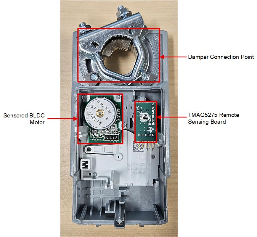 Figure 3-14 BLDC Damper Control Test Setup
One important note regarding the damper motor/gear is that the rotation to the left requires a higher current, while rotating to the right requires much less current. In this section, over to right (OTR) refers to the lower current rotation of the damper to the right while over to left represents the higher current rotation of the BLDC motor to the left.
A secondary TMAG5273 board is employed as a means of remotely detecting the damper position due to the size of the reference design and lack of mounting options for the board to the product. the TMAG5273 remote board is shown in Figure 3-15 below.
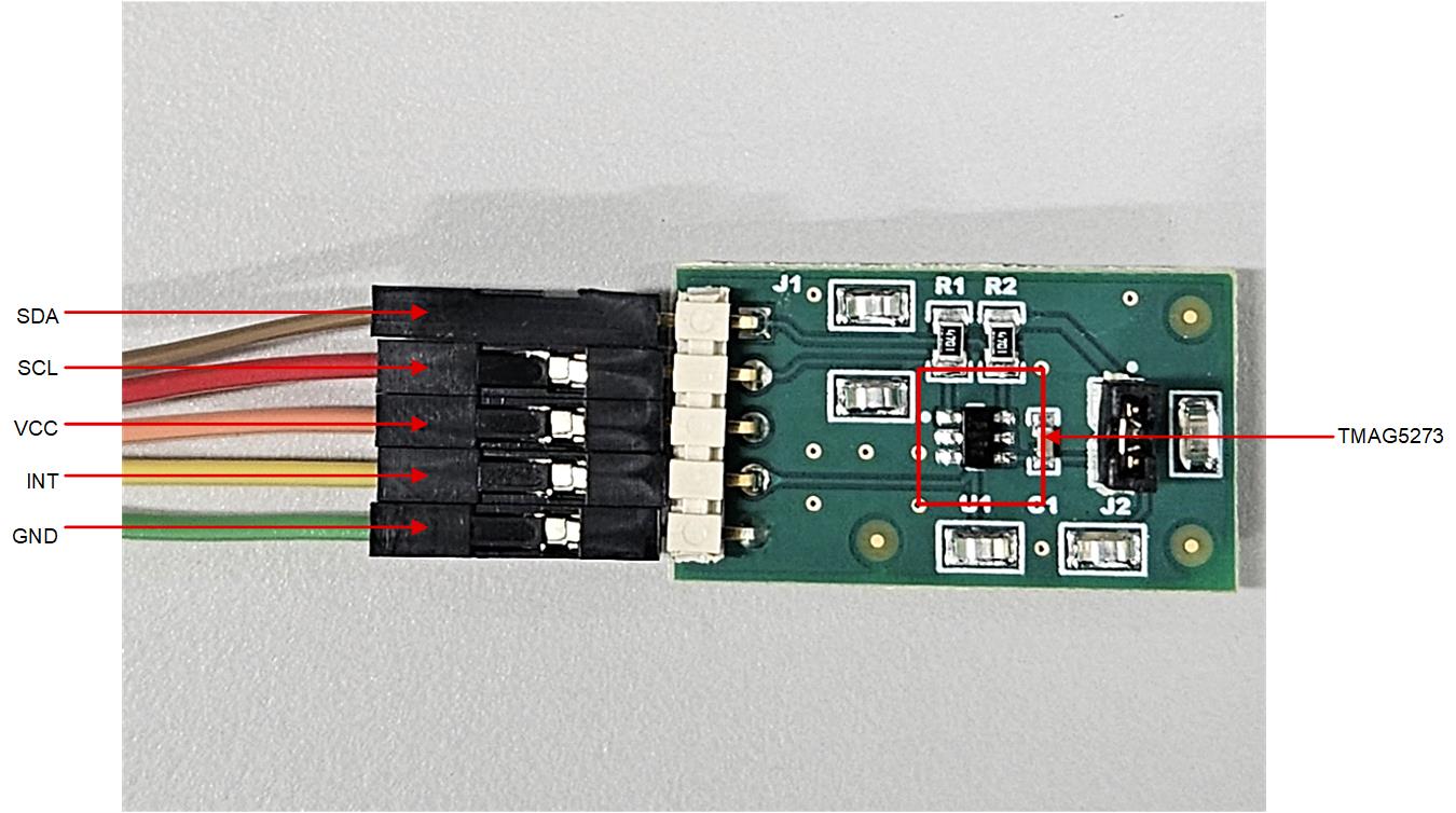 Figure 3-15 TMAG5273 Remote Sensing Board for BLDC Motor Position Sensing
Figure 3-16 below shows the motor voltage output on each of the 3 phases during OTL operation. The output to the BLDC motor is 120⁰ between each phase and the output voltage to the BLDC motor is ranges from 15.38V to 15.73V for each output phase.
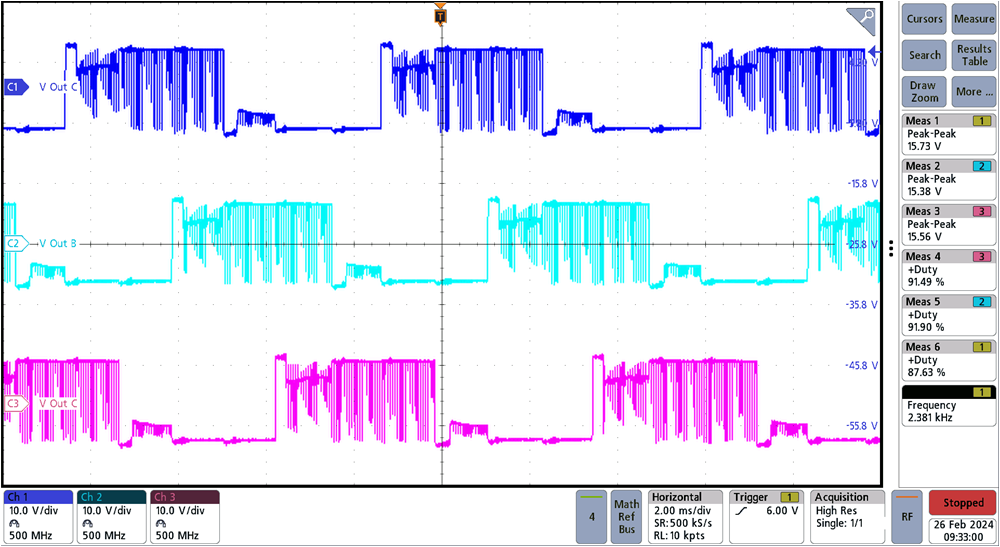 Figure 3-16 DRV8316C Voltage Output for Each Phase
DRV8316C phase current during operation: Figure 3-17 Below shows the output current for each phase of the BLDC motor during OTL operation. The phase current waveforms are 120 degrees between phase with a total RMS current of 474.6mA. The RMS current is captured during the high current rotation to the left.
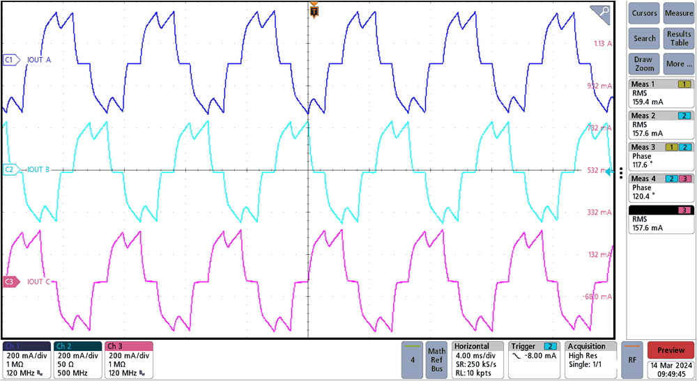 Figure 3-17 DRV8316C Output Current During Motor Operation
The waveform below in Figure 3-18 shows the current at the input to the DRV8316C during OTL operation of the BLDC motor. The current consumed by the DRV8316C peaks at approximately 187mA while driving the sensored BLDC motor apparatus with an RMS value of 190.1mA over the duration of movement. The Input voltage is AC coupled to extract the voltage ripple during operation. The voltage ripple is approximately 201mV during the high load rotation of the damper motor to the left.
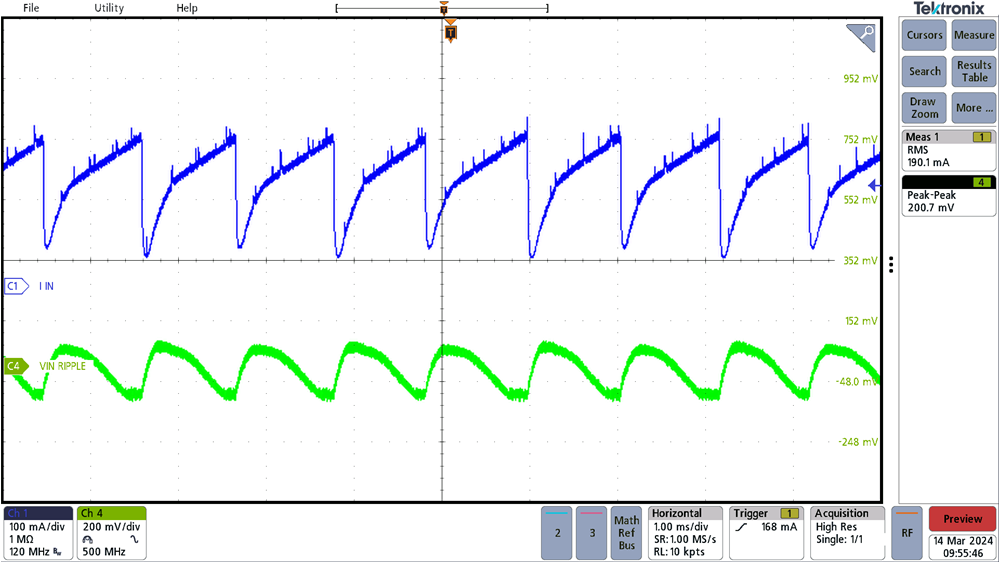 Figure 3-18 DRV8316C Input Current and Input Voltage Ripple During Operation
Figure 3-19 below shows the control signals from a single output phase of the MSPM0 (both INH and INL) as well as the current output from the SO pin during OTL operation.
The SOx pin on the DRV8316C outputs an analog voltage proportional to current flowing in the low side FETs multiplied by the gain setting (GCSA). The gain setting is adjustable between four different levels which can be set by the GAIN pin (in hardware device variant) or the GAIN bits (in SPI device variant). The current sense is implemented with the sense FET on each low-side FET of the DRV8316C device. This current information is fed to the internal I/V converter, which generates the CSA output voltage on the SOx pin based on the voltage on VREF pin and the Gain setting.
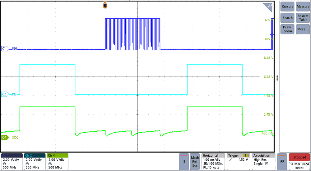 Figure 3-19 DRV8316C INH, INL, and SOx During Motor Operation (OTL)
Figure 3-20 shows the same outputs during the OTR operation. The INH and INL control signal along with the SOx are much shorter in duration with an increased frequency during the faster rotation of the damper motor in this scenario.
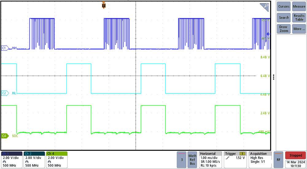 Figure 3-20 DRV8316C INH, INL, and SOx During Motor Operation (OTR)
DRV8428 Test Results
The DRV8428 testing is very similar to that of the BLDC damper motor, but instead leveraging a 24VDC bipolar stepper motor. A magnet is affixed to the back of the motor as shown below in Figure 3-21, and this is used for the position control loop in the case of 0V-10V or 4mA-20mA control, and simply as a position verification measure in the case the stepper motor is controlled by a temperature-based control loop.
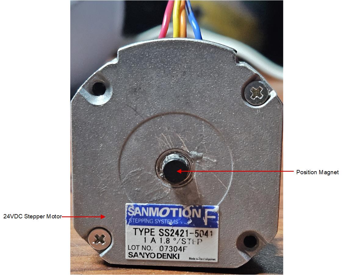 Figure 3-21 Stepper Motor Setup with Position Magnet
Figure 3-22 shows the load test results of the DRV8428 device driving a bipolar stepper motor in full stepping mode using a single-pin interface. In full-stepping mode, the full-bridge operates in either of two modes (forward or reverse mode) with a phase shift of 90° between the two windings. Figure 3-22 shows the STEP voltage, OUTA winding current, and OUT B winding.
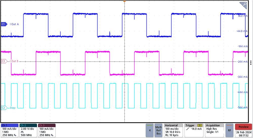 Figure 3-22 DRV8428 Phase Output and STEP Control Signal
DRV8428 Stepper Motor Drive efficiency:
To test the efficiency of the DRV8428, the input DC voltage to the device is swept from 15VDC to 24VDC while observing the current output of the power supply during operation. Current probes and voltage meters are used on each output from the DRV8316C during motor operation as well to acquire the RMS voltage and RMS current for each phase. The test is performed twice leveraging different decay mode settings to highlight the efficiency improvements that can be achieved.
Figure 3-23 below shows the current and voltage outputs for the DRV8428 during operation with the decay pin set to 0 through a GPIO from the MSPM0 (smart tune ripple control enabled). Smart tune Ripple Control operates by setting an IVALLEY level alongside the ITRIP level. When the current level reaches ITRIP, instead of entering slow decay until the tOFF time expires, the driver enters slow decay until IVALLEY is reached. Slow decay operates similar to mode 1 in which both low-side MOSFETs are turned on allowing the current to recirculate. In this mode, tOFF varies depending on the current level and operating conditions. This method allows much tighter regulation of the current level increasing motor efficiency and system performance. Smart tune Ripple Control can be used in systems that can tolerate a variable off-time regulation scheme to achieve small current ripple in the current regulation. The VREF pin is set to 1.5V from the MSPM0 DAC through firmware. The M0 pin of the DRV8428 is driven to 0, while the M1 pin is connected through a 330kΩ resistor to ground, setting the microstepping mode to full step (2-phase excitation) with 71% current.
The measured RMS voltage and current for AOUT 1 is 1.69V and 367.1mA RMS, and the BOUT 1 is 2.08V and 368.4mA respectively. The off-time for each phase is 9.86ms, and both outputs are 90 degrees phase shifted.
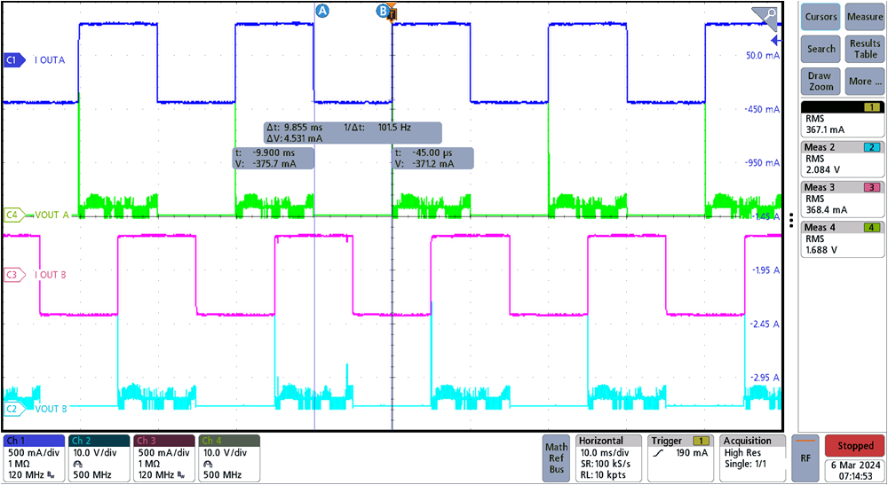 Figure 3-23 DRV8428 Output Current and Voltage with Smart Tune Ripple Control
Table 3-4 below shows the test results for the DRV8428 efficiency during operation with the decay mode set to smart tune ripple control. The input DC Power is gradually increased and the RMS output voltage/current is recorded to calculate the motor drive efficiency.
| DC Input Power | Output RMS Current | Efficiency |
|---|---|---|
| 1.85 | 721.10 | 71.93% |
| 1.89 | 714.80 | 75.04% |
| 1.93 | 715.00 | 74.39% |
| 1.93 | 717.40 | 74.73% |
| 2.01 | 717.30 | 72.98% |
| 2.03 | 718.70 | 72.85% |
| 2.05 | 719.90 | 72.98% |
| 2.07 | 723.00 | 73.19% |
| 2.10 | 725.10 | 73.61% |
| 2.11 | 726.20 | 74.78 |
Figure 3-24 below shows the resulting motor drive efficiency over the input DC power.
 Figure 3-24 DRV8428 Efficiency Over Input Power
For the second test, the decay mode is set to HI-Z which leverages the smart tune dynamic decay mode. This decay mode setting is optimized iteratively each PWM cycle. If the motor current overshoots the target trip level, then the decay mode becomes more aggressive (add fast decay percentage) on the next cycle to prevent regulation loss. If a long drive time must occur to reach the target trip level, the decay mode becomes less aggressive (remove fast decay percentage) on the next cycle to operate with less ripple and more efficiently. On falling steps, smart tune Dynamic Decay automatically switches to fast decay to reach the next step quickly. The VREF remains at 1.5V set with the MSPM0 DAC, utilizing full step 2 phase excitation with 71% current. Figure 3-25 below shows the output of both AOUT 1 and BOUT 1during motor operation. AOUT1 has an RMS voltage of 2.36V and an RMS current output of 317.4mA. For BOUT 1 the RMS voltage is 2.73V and RMS current is 320.1mA. The off-time in this mode is approximately 7.66ms.
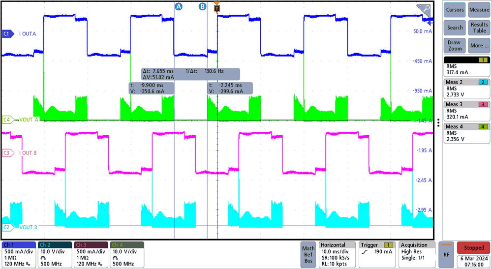 Figure 3-25 DRV8428 Output Current and Voltage With Smart Tune Dynamic Decay
Table 3-5 below shows the recorded data for each incremental input voltage value along with the calculated efficiency for each.
| DC Input Power (W) | Total Output RMS Current (mA) | Efficiency (%) |
|---|---|---|
| 1.54 | 671.80 | 77.05% |
| 1.59 | 671.50 | 75.54% |
| 1.59 | 667.30 | 79.74% |
| 1.60 | 666.90 | 83.52% |
| 1.61 | 660.20 | 84.14% |
| 1.62 | 656.20 | 88.61% |
| 1.62 | 650.40 | 91.88% |
| 1.63 | 646.10 | 94.34% |
| 1.65 | 639.90 | 95.42% |
| 1.68 | 636.80 | 96.96% |
Figure 3-26 below shows the efficiency and the total phase output current plots across the input power range for the DRV8428 with smart tune dynamic decay enabled. In this test, the efficiency numbers are considerably better and proportional to the input supply voltage, peaking at approximately 97% at 24VDC input voltage.
 Figure 3-26 DRV8428 Efficiency over Input Power