SBOA528 April 2022 OPA607
Design Goals
| Input | Output | Supply | ||||
|---|---|---|---|---|---|---|
| 2 VPP, 500 kHz Square wave |
Gain = 1 V/V | Vcc | Vee | Vref | ||
| 5 V | 0 V | 2.5 V | ||||
Design Description
A decompensated amplifier is defined as an amplifier that is not inherently stable below a minimum specified gain, but offers a higher gain bandwidth product (GBWP) and sometimes lower noise versus its unity-gain stable counterpart (see OPA858 versus OPA859). This circuit document presents three different external compensation methods for making these amplifiers unity-gain stable. Each circuit increases low gain stability at the expense of bandwidth. The first two circuits modify the amount-of-feedback (β) to increase the noise-gain (1/ β). The third circuit uses the output impedance of the amplifier in conjunction with an output load to attenuate the effective open-loop gain (AOL).
These examples stabilize the OPA607, a ≥ 6 V/V decompensated amplifier, in a unity-gain difference amplifier circuit.
Compensation Circuit 1: Differential Input Resistor (RIN)
 Circuit 1 Schematic
 Frequency Response
 Stability
Analysis") Noise-Gain (Amount of Feedback) Stability
Analysis
Noise-Gain (Amount of Feedback) Stability
AnalysisDesign Notes
Add a resistor (RIN) between the two
inputs that is small enough to decrease the amount-of-feedback (β) to
≤ 1/6, and increase the noise-gain (1/ β) to ≥ 6.
RIN does not affect the signal gain because of the virtual short
between the two inputs. This method increases the noise gain of the amplifier
uniformly across all frequencies, but sacrifices the least bandwidth.
Design Steps
In this difference amplifier circuit example, ΔV(RIN) is the voltage across resistor RIN in the circuit 1 schematic, and ΔV(OUT) is the voltage at Vout. β is the ratio ΔV(RIN) / ΔV(OUT) that is divided across the feedback. This ratio can be factored into:
First, the amount of ΔV(OUT) fed back to ΔV(IN–) across the feedback resistor RF is:
ZG represents the resistance out of IN–. To calculate ZG, add RIN to the resistance out of IN+, which is the parallel combination of R4 ll R5 ll R6. The result adds in parallel with the gain resistor RG at IN– to form ZG.
Second, because of the series resistance out of IN+, the voltage ΔV(RIN) is only a fraction of ΔV(IN–).
When RIN = ∞, β = 1/2 in this example circuit, where R4 ll R5 ll R6 = 500 Ω, RG= 1 kΩ, and RF= 1 kΩ. To stabilize the OPA607, set β = 1/6 and solve for RIN. This can also be solved with simulation, as shown in the noise-gain stability analysis image. RIN = 500 Ω raises the noise-gain up from 2 V/V to 6 V/V. A smaller RIN further increases 1/β.
Design Results
The silver peaking in the Frequency Response and ringing in the Square-Wave Response are signs of < 45° of phase margin and instability. Simulation and measurement of this circuit (see the following images) show that RIN = 499 Ω is sufficient for external compensation and stability. The higher undershoot shown is due to the faster falling edge slew rate of the OPA607.
 500 kHz, 2 Vpp Square-Wave Response
Compensation Circuit 2: Feedback Capacitor (CF)
 Circuit 2 Schematic
 Frequency Response
 Stability
Analysis") Noise-Gain (Amount of Feedback) Stability
Analysis
Noise-Gain (Amount of Feedback) Stability
AnalysisDesign Notes
Add a feedback capacitor (CF) which creates a high-frequency gain ≥ 6 V/V in conjunction with the amplifier input capacitance, but use RF / RG to set a lower signal gain at low frequency and DC. Ensure that the high-frequency noise-gain both is ≥ 6 V/V and is achieved within the gain-bandwidth of the amplifier. That is, in the noise-gain stability analysis image, the maroon AOL curve must intersect the olive 1/β (invBeta) curve where both the AOL curve is –20 dB/decade and the 1/β curve is flat versus frequency.
Design Steps
The high-frequency gain is set by a capacitor divider, formed between CF and the three parasitic input capacitances of the OPA607: CIN– = 5.5 pF; CIN+ = 5.5 pF; and CINDIFF = 11.5 pF. β is calculated with the same factors discussed in Circuit 1, but using these internal capacitors instead of external resistors.
In this noise-gain stability analysis, CF = 8.2 pF raises the high-frequency capacitor gain to 6.57 V/V. A smaller feedback capacitor further decreases β and increases the high-frequency gain.
This stable β suggests that the amplifier now has a signal gain ≥ 6 V/V at high frequency. But careful selection of both CF and RF values can create both a stable amount of feedback and also a low-pass filter of the signal gain, to prevent the increasing 1/β over frequency from creating issues like overshoot. It is easier to achieve both of these conditions when RF is > 10 kΩ.
Design Results
Measurement of this circuit shows that CF = 8.2 pF and RF = 13.7 kΩ were sufficient to both maintain a stable noise-gain = 6.57 V/V and filter overshoot.
 500 kHz, 2 Vpp Square-Wave Response
Compensation Circuit 3: High-Frequency Load (RISO)
 Circuit 3 Schematic
 Frequency Response
 Stability
Analysis") Noise-Gain (Amount of Feedback) Stability
Analysis
Noise-Gain (Amount of Feedback) Stability
AnalysisDesign Notes
Add a low-resistance load (RISO) for high frequencies. The load forms a resistor divider with the amplifier open-loop output impedance (see the following image), and can attenuate the effective open-loop gain (AOL) of the amplifier to a compensated level. Since the OPA607 has 500 Ω of series output impedance, a 100-Ω load resistor attenuates the AOL to 1/6 (–15.5 dB).
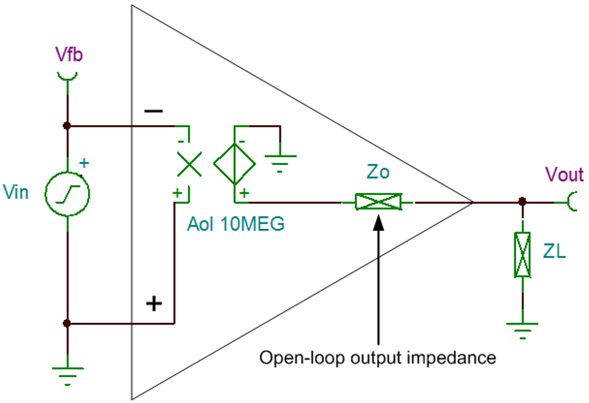
Alone, a small resistor load burns a lot of power. But for stability purposes, attenuating the AOL is like increasing the noise-gain, and only a high-frequency load is required, such as an output filter. In the noise-gain stability analysis circuit, both the black unloaded AOL and the maroon AOL with an RC filter load are graphed. The olive 2 V/V (6 dB) noise-gain intersects with the maroon loaded AOL at a more stable, 20-dB/decade rate of closure. This compensation technique is helpful for using the OPA607 as a drop-in replacement for unity-gain stable amplifiers where an output filter is present.
Design Steps
The RISO + CL filter bandwidth must be lower than the attenuated bandwidth of the loaded amplifier, because the frequency range above the filter bandwidth and below the loaded amplifier bandwidth is where the compensation is created. Otherwise, the load further decompensates the amplifier without creating a usable lower gain. In the stability analysis for this circuit, the –40 dB/decade slope in the maroon loaded AOL shows that higher gains will be less stable than the compensated low gain when a filter load attenuates the AOL.
In this example circuit, GBWP = 50 MHz and β = 1/2, but attenuation = 1/6. Therefore, the attenuated amplifier bandwidth is 50/12 = 4.2 MHz. For RISO = 100 Ω, CL should be > 380 pF.
Design Results
Measurement of this circuit shows that a RISO = 100 Ω, 470-pF load was sufficient to make the OPA607 stable in a difference configuration with a gain of 1 V/V.
 500 kHz, 2 Vpp Square-Wave Response
Design Featured Device
| OPA607 | |
|---|---|
| Supply Range (Vss) | 2.2 V to 5.5 V |
| Gain Bandwidth Product, G = 20 V/V | 50 MHz |
| Decompensated Gain (AV/V) | ≥ 6 V/V |
|
Input Capacitance (CIN) |
Differential: 11.5 pF |
| Common-mode: 5.5 pF | |
| Input Range (VCMVR) | (V–) to (V+) – 1.1 V |
| Output Range (Vout) | Rail to Rail |
|
Overdrive Recovery Time (tOR) |
300 ns |
|
Voltage Noise (eN) |
3.8 nV/√(Hz) |
| Offset Voltage (Vos) | ± 120 µV |
| Quiescent Current (Iq) | 900 µA |
| Input Bias Current (Ib) | ± 3 pA |
| Slew Rate | 24 V/µs |
|
Open-loop Output Impedance (Zo) |
500 Ω |
| OPA607 | |
Design Alternative Devices
| Decompensated High-Speed Amplifiers | ||
|---|---|---|
| Device Name | Gain Bandwidth | Decompensated Gain |
| LMV793, LMV794 LMP7717, LMP7718 |
88 MHz | 10 V/V |
| SM73302 | 88 MHz | 10 V/V |
| OPA838 | 300 MHz | 6 V/V |
| LMH6629 | 900 MHz | 10 V/V |
| LMH6626 | 1.5 GHz | 10 V/V |
| OPA818 | 2.7 GHz | 7 V/V |
| OPA858 | 5.5 GHz | 7 V/V |
Design References
- See the Analog Engineer's Circuit Cookbooks for TI's comprehensive circuit library.
- Texas Instruments, AN-1604 Decompensated Operational Amplifiers application note
- For hardware evaluation, see TIDA-060019
Additional Resources
- Texas Instruments, OPAx607 50-MHz, Low-Power, Rail-to-Rail Output CMOS Operational Amplifier for Cost Sensitive Systems data sheet