SNAA363 May 2022 ADC128S102-SEP
1 Application Brief
Design Description
This application brief demonstrates voltage-sensing circuits using a simple voltage divider with the ADC128S102-SEP, which is a radiation-tolerant, low-power, eight-channel, 50-kSPS to 1-MSPS, 12-bit analog-to-digital converter (ADC). This product is similar to the ADC128S102QML-SP, which is a radiation-hardened version of this ADC that has been in the market since 2008. In comparison, the ADC128S102-SEP has lower radiation performance with TID = 30 krad (Si), and is a lower cost, smaller size ADC designed for low-Earth orbit (LEO) applications.
The analog front end of this sensing circuit is designed in two different versions. Circuit 1 is designed to run at 50 kSPS or higher with sampled signal error less than 1/2 of LSB. Circuit 2 is designed to maximize power savings but runs at lower speed with sampled signal error less than 1 LSB. Both circuits use the TPS73801-SEP, a radiation-tolerant LDO regulator, as a 5-V reference voltage for the ADC for all error calculations.
Circuit 1 Schematic
50-kSPS Voltage Sensing Circuit shows the example circuit used throughout this document, it is a voltage sensing circuit without the use of an op-amp input buffer. The input signal is divided down from 15 V to 4.5 V at the ADC input. The ADC simulations run at 50 kSPS with a conversion transient settling error of 1/2 of LSB. Using a 5-V reference to set the full-scale range, the target error is less than 610.4 μV. This is a DC error, which in addition to many other DC errors, results in the total error.
Sampling a single-channel at a higher-than-required sampling rate allows the user to average samples to increase the SNR of the system. Noise performance improves equal to the SQRT(N) samples averaged.
 50-kSPS Voltage Sensing Circuit
Circuit 1 Design Steps
- Calculate R1, R2, and Cfilt value using the ADC Drive Without Amplifier section in the Analog Engineer's Calculator. A calculation example follows. To complete the calculation, the tool needs the following information:
- Sample and hold capacitance (Csh), which is shown as Cin in the data sheet
- Vin and Vadc for setting the R1 and R2 ratio
- Sampling rate, which is 50 kSPS in this case for maximum power saving
- To achieve 50-kSPS sampling rate, the digital clock input (sclk) is 800 kHz. Conversion time (tconv) is 13 clock cycles, which is calculated to be 16.25 μs.
- ADC resolution is 12 bits
 R1, R2, and Cfilt Calculation in Analog Engineer's Calculator - Supply Monitor
 - Simulate in TINA-TI SPICE to measure the sampled signal settling time to confirm it indeed settled within the acquisition time (tacq).
Circuit 1 Simulation Result
Based on previous calculation, a TINA-TI SPICE simulation was created. The sample rate is set to 50 kSPS, an input voltage signal of 15 V is divided down to 4.5 V.
The ADC output measurement is compared to the ideal input signal using a Verror multimeter, this reading demonstrates if the target error of 1/2 of LSB is achieved within the acquisition time.
 50-kSPS Voltage-Sensing Circuit Schematic in TINA-TI SPICE
 50-kSPS Voltage-Sensing Circuit Simulation Result in TINA-TI SPICE
The simulation result in 50-kSPS Voltage-Sensing Circuit Simulation Result in TINA-TI SPICE shows that the sampled signal settles at 402 μV at the end of the acquisition time, which is far less than 1/2 of the LSB. Notice that the input is a DC signal, if an AC signal is used instead a different analysis method is required to properly analyze the settling behavior.
Circuit 2 Schematic
0.25-kSPS Low-Power Voltage-Sensing Circuit Without Using Buffer shows the circuit 2 schematic. This circuit is similar to circuit 1 except that R1 and R2 are increased to save power and Cfilt is increased to supply more current to Csh.
 0.25-kSPS Low-Power Voltage-Sensing Circuit Without Using Buffer
Circuit 2 Design Steps
1. Determine R1, R2, and Cfilt using the following equations: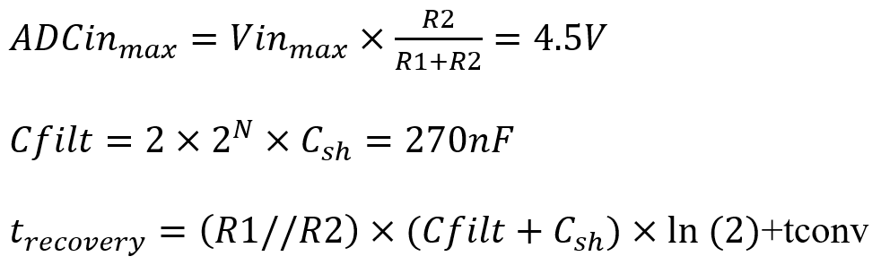
where
- ADCin is the voltage input of the ADC128S102-SEP
- Vinmax is the upper range of sensing voltage, which is 15 V
- ADCinmax is the upper range of ADCin, which is 4.5 V
- N is the number of bits
- Csh is 33 pF from the ADC128S102-SEP data sheet
These calculations can also be completed in the ADC Drive Without Amplifier section in the Analog Engineer's Calculator.
 Recovery Time and Cfilt Calculation in Analog Engineer's Calculator - Periodic Single Shot
In the calculation displayed in the previous image, tconv(max) is 16.25 μs when ADC is sampling at 50 kSPS. Csh is set to 33 pF, and Rin, which is equal to R1//R2, is 21 kΩ if R1 and R2 are 70 kΩ and 30 kΩ. The calculation result shows the minimum recovery time is 3.952 ms and Cfilt is 270.3 nF.
2. Simulate in TINA-TI SPICE to confirm Cfilt is settled before acquisition time and measure the sampled signal errorCircuit 2 Simulation Result
Choosing R1 and R2 to be 70 kΩ and 30 kΩ, and Cfilt, the charge bucket capacitor, to be 270 nF, circuit 2 simulation is set up such that the ADC is operated in a single-shot mode where the voltage input channel is only measured once every 4 ms, or 250 Hz. This mode of operation is common if certain channels are sampled repeatedly at a higher sampling rate while other monitoring channels are only occasionally selected with the MUX and converted.
 0.25-kSPS Low-Power Voltage Sensing Circuit Error Simulation in TINA-TI SPICE
As shown in the previous simulation result, the error ends up at the sampled signal is about 1.085 mV, which is smaller than 1 LSB, 1.221 mV, yielding a 0.024% error.
 0.25-kSPS Low-Power Voltage Sensing Circuit Charge Bucket Simulation in TINA-TI SPICE
ADCin is the Cfilt voltage and Vacq is the acquisition on and off switch at the sample and hold circuit. In circuit 2, Csh is charged mainly by the Cfilt. After Vacq turns back to low, DACin begins to be charged and it takes about 4 ms for the Cfilt to be charged from 1 LSB below 4.5 V up to 1/2 LSB below 4.5 V. This indicates the signal can be sampled at a highest rate of 250 Hz.
Error Calculation
The previous simulations were used to determine the transient settling error and do not include error caused by the voltage divider and temperature drift. To calculate the circuit error, use the following formulas and the TUE Calculator section in the Analog Engineer's Calculator.
- R1tol: R1 resistor tolerance [%]
- TC1: R1 Resistor temperature coefficient [ppm/C]
- R2tol: R2 resistor tolerance [%]
- TC2: R2 Resistor temperature coefficient [ppm/C]
- Ileak: ADC128S102-SEP Input leakage current
Gain error, eR1 and eR2 [%], caused by resistor tolerance and temperature drift:
Offset error, eleakCurr [%], caused by Ileak, which is 1 μV found in the ADC128S102-SEP data sheet:
Error introduced by ADC128S102-SEP and TPS73801-SEP, which is used to provide the 5-V reference voltage to pin VA of ADC128S102-SEP, can be calculated using the TUE Calculator in the Analog Engineer's Calculator. To use the calculator, input the values listed in the screen from the device data sheet:
 TUE Calculation, Displaying ADC Specifications and Non-calibrated Results
 TUE Calculation, Displaying LDO Specifications and Calibrated Results
The TUE calculator was used to solve for the Total Unadjusted Error of the system. TUE Calculation, Displaying ADC Specifications and Non-calibrated Results displays the ADC error tab with the values input from the ADC128S102-SEP data sheet, while TUE Calculation, Displaying LDO Specifications and Calibrated Results displays the Reference Error tab with the values input from the TPS73801-SEP data sheet. Fill in both of these tabs for an accurate TUE result. Note that the amplifier Error tab is not used in this example. The Analog Engineer's Calculator provides results using various calibration options, under Analysis Options.
The previous two images display the non-calibrated results and the results with Gain and Offset calibrated, respectively. With temperature ranges from –55°C to 125°C, calculations show that ADC128S102-SEP and TPS73801-SEP contribute around 1.35% typical error and 2.68% maximum error without calibration, and 0.1636% typical error and 0.1660% maximum error with both gain and offset calibration.
Conclusion
ADC128S102-SEP has excellent performance on voltage measurement with a simple voltage divider. Circuits 1 and 2 can also be turned into temperature-sensing circuits by simply replacing one of the voltage divider resistors with an NTC or PTC thermistor. In applications, such as RF power amplifier biasing, motor driving, telemetry, electric cooler control, battery charging, and so forth, the use of ADC128S102-SEP can reduce cost and circuit size by removing buffers in all voltage sensing rails. In addition, TI has op amps, such as OPA4H014-SEP, an 11-MHz high-precision amplifier that can be used as a buffer for driving this ADC for a higher sampling rate. The Radiation-Tolerant, 30-krad, Comparing Current Sensing Amplifier With Second Stage Buffer to ADC circuit document demonstrates a current sensing circuit that drives ADC128S102-SEP with OPA4H014-SEP.
For more op-amp options, refer to the TI Space Product Guide.