SNVSA02A January 2016 – December 2016 LM5140-Q1
PRODUCTION DATA.
- 1 Features
- 2 Applications
- 3 Description
- 4 Revision History
- 5 Pin Configuration and Functions
- 6 Specifications
-
7 Detailed Description
- 7.1 Overview
- 7.2 Functional Block Diagram
- 7.3
Feature Description
- 7.3.1 High Voltage Start-up Regulator
- 7.3.2 VCC Regulator
- 7.3.3 Oscillator
- 7.3.4 SYNIN and SYNOUT
- 7.3.5 Enable
- 7.3.6 Power Good
- 7.3.7 Output Voltage
- 7.3.8 Minimum Output Voltage Adjustment
- 7.3.9 Current Sense
- 7.3.10 DCR Current Sensing
- 7.3.11 Error Amplifier and PWM Comparator
- 7.3.12 Slope Compensation
- 7.4 Device Functional Modes
- 8 Application and Implementation
- 9 Power Supply Recommendations
- 10Layout
- 11Device and Documentation Support
- 12Mechanical, Packaging, and Orderable Information
Package Options
Mechanical Data (Package|Pins)
- RWG|40
Thermal pad, mechanical data (Package|Pins)
Orderable Information
1 Features
- Qualified for Automotive Applications
- AEC-Q100 Test Guidance With the Following
- Device Temperature Grade 1: –40ºC to +125ºC Ambient Operating Temperature
- Device HBM ESD Classification Level 2
- Device CDM ESD Classification Level C4B
- Input Operating Range from 3.8 V to 65 V (70 V Absolute Maximum)
- Two Interleaved Buck Controllers With:
- VOUT1 Fixed 3.3 V, 5 V, or Adjustable
from 1.5 V – 15 V, Accuracy ±1% - VOUT2 Fixed 5 V, 8 V, or Adjustable
from 1.5 V – 15 V, Accuracy ±1%
- VOUT1 Fixed 3.3 V, 5 V, or Adjustable
- Fixed 2.2-MHz or 440-kHz Switching Frequency, Accuracy ±7%
- Optional Synchronization to an External Clock
- SYNC Output Clock for Additional Converters
- Shutdown Mode Current: 9 µA Typical
- No Load Standby Current: 35 µA Typical (One Channel Operating)
- Current Limit Threshold Programmable to 50 mV or 75 mV, Accuracy ±10%
- Independent Enable Inputs for VOUT1 and VOUT2
- Hiccup Mode Protection for Sustained Overload
- Independent Power Good Outputs
- High-Side and Low-Side Gate Drivers With Adjustable Slew Rate Control
- Selectable Diode Emulation or Continuous Conduction at Light Load
- 40-Pin VQFN Package With Wettable Flanks
2 Applications
- Automotive Electronics
- Infotainment Systems
- Instrument Clusters
- Advanced Driver Assistance (ADAS)
3 Description
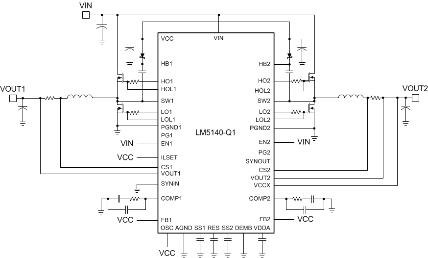
The LM5140-Q1 is a dual synchronous buck controller intended for high voltage wide VIN step-down converter applications. The control method is based on current mode control. Current mode control provides inherent line feedforward, cycle-by-cycle current limiting, and easier loop compensation.
The LM5140-Q1 features adjustable slew rate control to simplify compliance with the CISPR and automotive EMI requirements. The LM5140-Q1 operates at selectable switching frequencies of 2.2 MHz or 440 kHz with the two controller channels switching 180º out of phase. In light or no-load conditions, the LM5140-Q1 operates in skip cycle mode for improved low power efficiency. The LM5140-Q1 includes a high voltage bias regulator with automatic switchover to an external bias supply to improve efficiency and reduce input current. Additional features include frequency synchronization, cycle-by-cycle current limit, hiccup mode fault protection for sustained overloads, independent power good outputs, and independent enable inputs.
Device Information(1)
| PART NUMBER | PACKAGE | BODY SIZE (NOM) |
|---|---|---|
| LM5140-Q1 | VQFN (40) | 6.00 mm × 6.00 mm |
- For all available packages, see the orderable addendum at the end of the data sheet.
Simplified Schematic
