SNAS548D February 2000 – January 2015 LM555
PRODUCTION DATA.
- 1 Features
- 2 Applications
- 3 Description
- 4 Revision History
- 5 Pin Configuration and Functions
- 6 Specifications
- 7 Detailed Description
- 8 Application and Implementation
- 9 Power Supply Recommendations
- 10Layout
- 11Device and Documentation Support
- 12Mechanical, Packaging, and Orderable Information
Package Options
Mechanical Data (Package|Pins)
Thermal pad, mechanical data (Package|Pins)
Orderable Information
1 Features
- Direct Replacement for SE555/NE555
- Timing from Microseconds through Hours
- Operates in Both Astable and Monostable Modes
- Adjustable Duty Cycle
- Output Can Source or Sink 200 mA
- Output and Supply TTL Compatible
- Temperature Stability Better than 0.005% per °C
- Normally On and Normally Off Output
- Available in 8-pin VSSOP Package
2 Applications
- Precision Timing
- Pulse Generation
- Sequential Timing
- Time Delay Generation
- Pulse Width Modulation
- Pulse Position Modulation
- Linear Ramp Generator
3 Description
The LM555 is a highly stable device for generating accurate time delays or oscillation. Additional terminals are provided for triggering or resetting if desired. In the time delay mode of operation, the time is precisely controlled by one external resistor and capacitor. For a stable operation as an oscillator, the free running frequency and duty cycle are accurately controlled with two external resistors and one capacitor. The circuit may be triggered and reset on falling waveforms, and the output circuit can source or sink up to 200 mA or drive TTL circuits.
Device Information(1)
| PART NUMBER | PACKAGE | BODY SIZE (NOM) |
|---|---|---|
| LM555 | SOIC (8) | 4.90 mm × 3.91 mm |
| PDIP (8) | 9.81 mm × 6.35 mm | |
| VSSOP (8) | 3.00 mm × 3.00 mm |
- For all available packages, see the orderable addendum at the end of the datasheet.
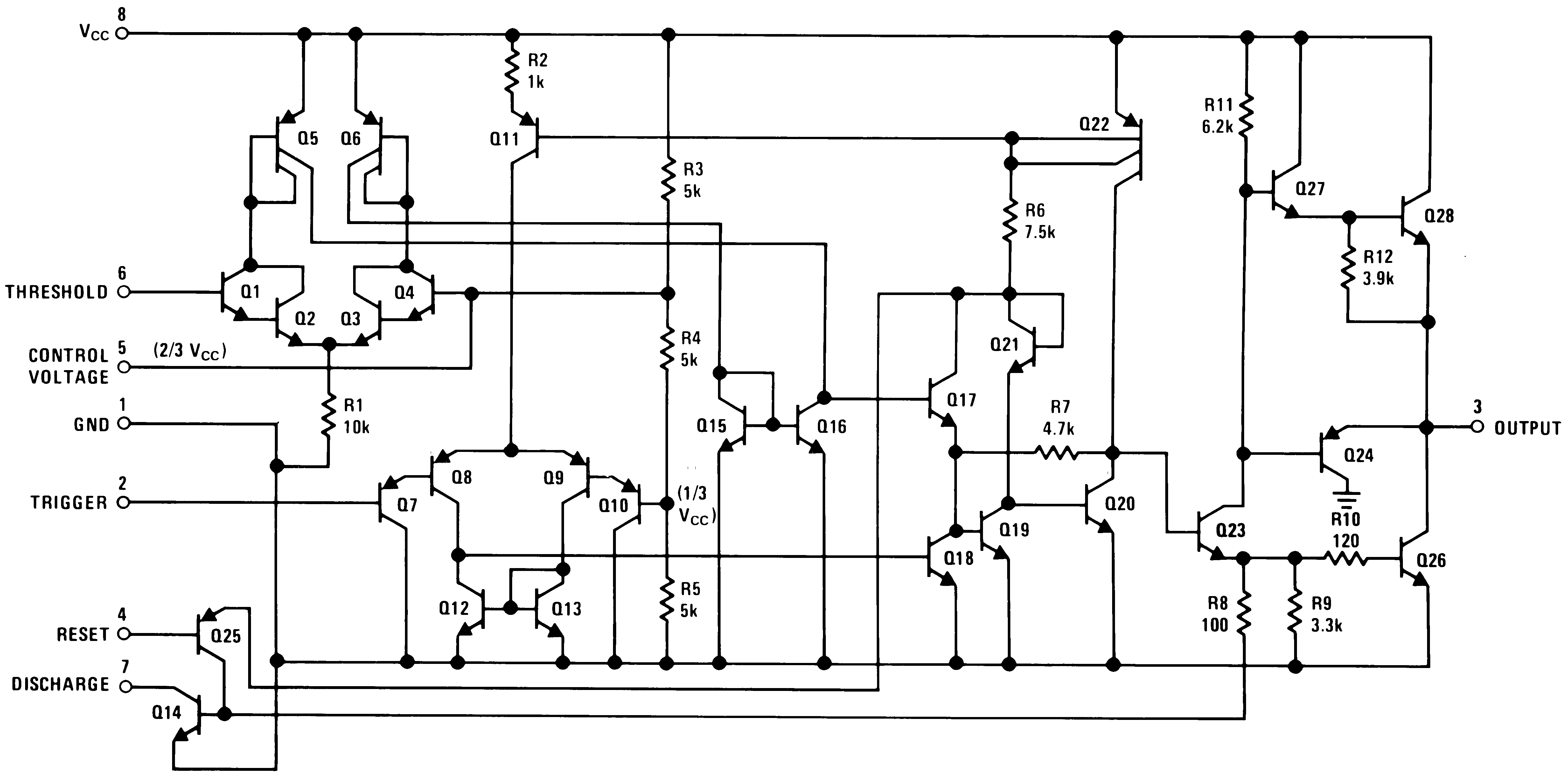
Schematic Diagram