SNAS252S October 2005 – December 2014 LMX2531
PRODUCTION DATA.
- 1 Features
- 2 Applications
- 3 Description
- 4 Revision History
- 5 Pin Configuration and Functions
- 6 Specifications
-
7 Detailed Description
- 7.1 Overview
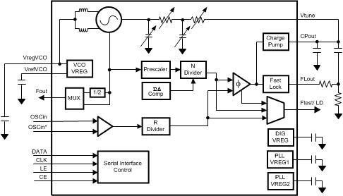
- 7.2 Functional Block Diagram
- 7.3 Feature Description
- 7.4 Device Functional Modes
- 7.5 Programming
- 7.6
Register Maps
- 7.6.1
General Programming Information
- 7.6.1.1 Initialization Sequence
- 7.6.1.2 Complete Register Content Map
- 7.6.1.3 Register R0
- 7.6.1.4 Register R1
- 7.6.1.5 Register R2
- 7.6.1.6 Register R3
- 7.6.1.7 Register R4
- 7.6.1.8
Register R5
- 7.6.1.8.1 EN_PLL -- Enable Bit for PLL
- 7.6.1.8.2 EN_VCO -- Enable Bit for the VCO
- 7.6.1.8.3 EN_OSC -- Enable Bit for the Oscillator Inverter
- 7.6.1.8.4 EN_VCOLDO -- Enable Bit for the VCO LDO
- 7.6.1.8.5 EN_PLLLDO1 -- Enable Bit for the PLL LDO 1
- 7.6.1.8.6 EN_PLLLDO2 -- Enable Bit for the PLL LDO 2
- 7.6.1.8.7 EN_DIGLDO -- Enable Bit for the digital LDO
- 7.6.1.8.8 REG_RST -- Resets All Registers to Default Settings
- 7.6.1.9
Register R6
- 7.6.1.9.1 C3_C4_ADJ[2:0] -- Value FOR C3 and C4 In The Internal Loop Filter
- 7.6.1.9.2 R3_ADJ_FL[1:0] -- Value for Internal Loop Filter Resistor R3 During Fastlock
- 7.6.1.9.3 R3_ADJ[1:0] -- Value for Internal Loop Filter Resistor R3
- 7.6.1.9.4 R4_ADJ_FL[1:0] -- Value for Internal Loop Filter Resistor R4 During Fastlock
- 7.6.1.9.5 R4_ADJ[1:0] -- Value for Internal Loop Filter Resistor R4
- 7.6.1.9.6 EN_LPFLTR-- Enable for Partially Integrated Internal Loop Filter
- 7.6.1.9.7 VCO_ACI_SEL
- 7.6.1.9.8 XTLSEL[2:0] -- OSCin Select
- 7.6.1.10 Register R7
- 7.6.1.11 Register R8
- 7.6.1.12 Register R9
- 7.6.1.13 Register R12
- 7.6.1
General Programming Information
- 8 Application and Implementation
- 9 Power Supply Recommendations
- 10Layout
- 11Device and Documentation Support
- 12Mechanical, Packaging, and Orderable Information
Package Options
Mechanical Data (Package|Pins)
Thermal pad, mechanical data (Package|Pins)
Orderable Information
1 Features
- Multiple Frequency Options Available
- See Device Information Table
- Frequencies From: 553 MHz to 3132 MHz
- PLL Features
- Fractional-N Delta-Sigma Modulator Order Programmable up to Fourth Order
- FastLock/Cycle Slip Reduction with Timeout Counter
- Partially Integrated, Adjustable Loop Filter
- Very Low Phase Noise and Spurs
- VCO Features
- Integrated Tank Inductor
- Low Phase Noise
- Other Features
2 Applications
- Cellular Base Stations
- Wireless LANs
- Broadband Wireless Access
- Satellite Communications
- Wireless Radios
- Automotive
- CATV Equipment
- Instrumentation and Test Equipment
- RFID Readers
- Data Converter Clocking
3 Description
The LMX2531 is a low-power, high-performance frequency synthesizer system which includes a fully integrated delta-sigma PLL and VCO with fully integrated tank circuit. The third and fourth poles are also integrated and adjustable. Ultra-low noise and high-precision LDOs are integrated for the PLL and VCO, which yield higher supply-noise immunity and more consistent performance. When combined with a high-quality reference oscillator, the LMX2531 device generates very stable, low-noise local-oscillator signals for up and down conversion in wireless communication devices. The LMX2531 device is a monolithic integrated circuit, fabricated in an advanced BiCMOS process. Several different versions of this product accommodate different frequency bands.
Device Information(1)
| PART | LOW BAND | HIGH BAND |
|---|---|---|
| LMX2531LQ1146E | 553 — 592 MHz | 1106 — 1184 MHz |
| LMX2531LQ1226E | 592 — 634 MHz | 1184 — 1268 MHz |
| LMX2531LQ1312E | 634 — 680 MHz | 1268 — 1360 MHz |
| LMX2531LQ1415E | 680 — 735 MHz | 1360 — 1470 MHz |
| LMX2531LQ1500E | 749.5 — 755 MHz | 1499 — 1510 MHz |
| LMX2531LQ1515E | 725 — 790 MHz | 1450 — 1580 MHz |
| LMX2531LQ1570E | 765 — 818 MHz | 1530 — 1636 MHz |
| LMX2531LQ1650E | 795 — 850 MHz | 1590 — 1700 MHz |
| LMX2531LQ1700E | 831 — 885 MHz | 1662 — 1770 MHz |
| LMX2531LQ1742 | 880 — 933 MHz | 1760 — 1866 MHz |
| LMX2531LQ1778E | 863 — 920 MHz | 1726 — 1840 MHz |
| LMX2531LQ1910E | 917 — 1014 MHz | 1834 — 2028 MHz |
| LMX2531LQ2080E | 952 — 1137 MHz | 1904 — 2274 MHz |
| LMX2531LQ2265E | 1089 — 1200 MHz | 2178 — 2400 MHz |
| LMX2531LQ2570E | 1168 — 1395 MHz | 2336 — 2790 MHz |
| LMX2531LQ2820E | 1355 — 1462 MHz | 2710 — 2925 MHz |
| LMX2531LQ3010E | 1455 — 1566 MHz | 2910 — 3132 MHz |
- For all available packages, see the orderable addendum at the end of the datasheet.
Simplified Schematic