SNAS252S October 2005 – December 2014 LMX2531
PRODUCTION DATA.
- 1 Features
- 2 Applications
- 3 Description
- 4 Revision History
- 5 Pin Configuration and Functions
- 6 Specifications
-
7 Detailed Description
- 7.1 Overview
- 7.2 Functional Block Diagram
- 7.3 Feature Description
- 7.4 Device Functional Modes
- 7.5 Programming
- 7.6
Register Maps
- 7.6.1
General Programming Information
- 7.6.1.1 Initialization Sequence
- 7.6.1.2 Complete Register Content Map
- 7.6.1.3 Register R0
- 7.6.1.4 Register R1
- 7.6.1.5 Register R2
- 7.6.1.6 Register R3
- 7.6.1.7 Register R4
- 7.6.1.8
Register R5
- 7.6.1.8.1 EN_PLL -- Enable Bit for PLL
- 7.6.1.8.2 EN_VCO -- Enable Bit for the VCO
- 7.6.1.8.3 EN_OSC -- Enable Bit for the Oscillator Inverter
- 7.6.1.8.4 EN_VCOLDO -- Enable Bit for the VCO LDO
- 7.6.1.8.5 EN_PLLLDO1 -- Enable Bit for the PLL LDO 1
- 7.6.1.8.6 EN_PLLLDO2 -- Enable Bit for the PLL LDO 2
- 7.6.1.8.7 EN_DIGLDO -- Enable Bit for the digital LDO
- 7.6.1.8.8 REG_RST -- Resets All Registers to Default Settings
- 7.6.1.9
Register R6
- 7.6.1.9.1 C3_C4_ADJ[2:0] -- Value FOR C3 and C4 In The Internal Loop Filter
- 7.6.1.9.2 R3_ADJ_FL[1:0] -- Value for Internal Loop Filter Resistor R3 During Fastlock
- 7.6.1.9.3 R3_ADJ[1:0] -- Value for Internal Loop Filter Resistor R3
- 7.6.1.9.4 R4_ADJ_FL[1:0] -- Value for Internal Loop Filter Resistor R4 During Fastlock
- 7.6.1.9.5 R4_ADJ[1:0] -- Value for Internal Loop Filter Resistor R4
- 7.6.1.9.6 EN_LPFLTR-- Enable for Partially Integrated Internal Loop Filter
- 7.6.1.9.7 VCO_ACI_SEL
- 7.6.1.9.8 XTLSEL[2:0] -- OSCin Select
- 7.6.1.10 Register R7
- 7.6.1.11 Register R8
- 7.6.1.12 Register R9
- 7.6.1.13 Register R12
- 7.6.1
General Programming Information
- 8 Application and Implementation
- 9 Power Supply Recommendations
- 10Layout
- 11Device and Documentation Support
- 12Mechanical, Packaging, and Orderable Information
Package Options
Mechanical Data (Package|Pins)
Thermal pad, mechanical data (Package|Pins)
Orderable Information
8 Application and Implementation
NOTE
Information in the following applications sections is not part of the TI component specification, and TI does not warrant its accuracy or completeness. TI’s customers are responsible for determining suitability of components for their purposes. Customers should validate and test their design implementation to confirm system functionality.
8.1 Application Information
The LMX2531 can be used in a broad class of applications. In general, they tend to fall in the categories where the output frequency is a nicely related input frequency and those that require fractional mode. The following schematic generally applies to most applications.
8.2 Typical Application
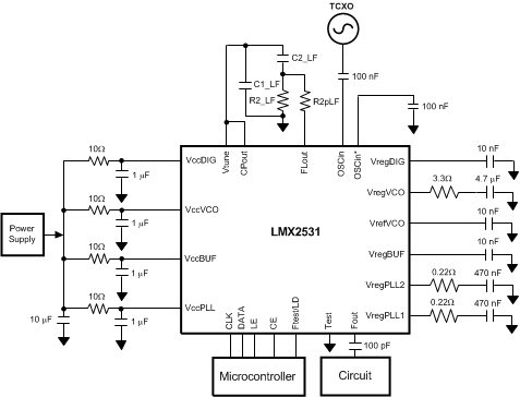
Table 30. Typical Connection Diagram
| PIN(S) | APPLICATION INFORMATION |
|---|---|
| Vcc, Vreg, and Vref Pins | Consult the power supply recommendations for these pins. |
| CLK DATA LE |
Because the maximum voltage on these pins is less than the minimum Vcc voltage, level shifting may be required if the output voltage of the microcontroller is too high. This can be accomplished with a resistive divider. |
| CE | As with the CLK, DATA, and LE pins, level shifting may be required if the output voltage of the microcontroller is too high. A resistive divider or a series diode are two ways to accomplish this. The diode has the advantage that no current flows through it when the chip is powered down. |
| Ftest/LD | It is an option to use the lock detect information from this pin. |
| Fout | This is the high frequency output. This needs to be AC coupled, and matching may also be required. The value of the DC blocking capacitor may be changed, depending on the output frequency. |
| CPout Vtune |
In most cases, it is sufficient to short these together, although there always the option of adding additional poles. C1_LF, C2_LF, and R2_LF are used in conjunction with the internal loop filter to make a fourth order loop filter. |
| R2pLF | This is the fastlock resistor, which can be useful in many cases, because the spurs are often better with low charge pump currents, and the internal loop filter can be adjusted during fastlock. |
| OSCin | This is the reference oscillator input pin. It needs to be AC coupled. |
| OSCin* | If the device is being driven single-ended, this pin needs to be shunted to ground with a capacitor. |
8.2.1 Design Requirements
Consider generating 1500-MHz fixed frequency from a fixed 10-MHz input frequency. This is the situation similar that was used for the LMX2531LQ1500E evaluation board.
For this design example, use the parameters listed in Table 31 as the user-input parameters.
Table 31. Design Procedure
| PARAMETER | VALUE | REASON FOR CHOOSING |
|---|---|---|
| Fout | 1500 MHz | This value was given. |
| Fosc | 10 MHz | This value was given. |
| Fpd | 10 MHz | This maximized for the best phase noise performance. This is an integer PLL design, so it makes sense to maximize this. If Fpd 10 MHz it was a fractional design, then sometimes lowering this frequency can improve fractional spurs. |
| Loop Bandwidth | 11.5 kHz | This is wider for better jitter, but it is also restricted by the internal loop filter |
| Phase Margin | 76.8 deg | Choosing a high phase margin is good for better jitter. |
| Kpd | 16x | Higher charge pump gains are better for better PLL phase noise |
| C3_LF | 50 pF | In general, the internal loop filter restricts how wide the loop bandwidth can be. Although a wider loop bandwidth could be obtained by switching out the internal loop filter altogether, it is nice to have some internal poles to filter some unwanted spurs. So this is the minimum setting for the internal loop filter. |
| C4_LF | 50 pF | |
| R3_LF | 10 kΩ | |
| R4_LF | 10 kΩ | |
| C1_LF | Open | The internal loop filter restricts the loop bandwidth. By making C1_LF=open, this maximizes the achievable bandwidth for a particular setup condition. |
| C2_LF | 82 nF | These can be calculated with the Clock Architect. |
| R2_LF | 1.5 kΩ | These can be calculated with the Clock Architect. |
| ORDER | "Reset Modulator" | The device should be set to integer mode. |
| DITHER | "Disabled" | Dithering does not help in integer mode. |
| XTLMAN | 80 | This is a setting for the LMX2531LQ1500E for a 10 MHz input. |
8.2.2 Detailed Design Procedure
Use the WEBENCH® Clock Architect to calculate the values of C2_LF and R2_LF.
Set the device to integer mode and DITHER to disabled.
8.2.3 Application Curves
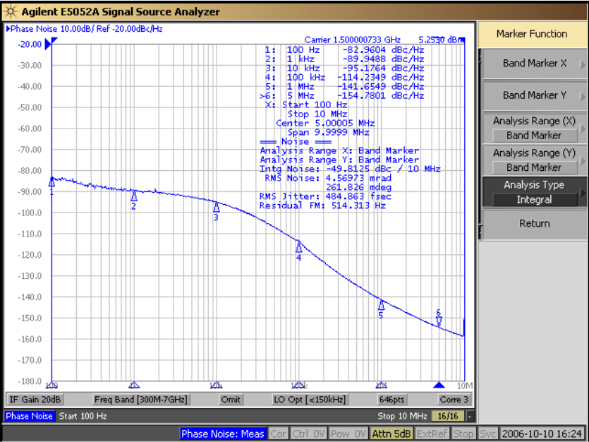 Figure 3. Closed Loop Phase Noise
 Figure 4. Open Loop VCO Noise
8.3 Do's and Don'ts
| Category | Do | Don't | Why |
|---|---|---|---|
| Loop Filter Design | For integer Designs: Maximize charge pump current and phase detector frequency. |
For Fractional Designs: Blindly maximize charge pump current and phase detector frequency. |
Maximizing the charge pump current and phase detector frequency give the best PLL phase noise and also allow a wider bandwidth with the internal filter engaged. However, increasing these also increase the integer boundary spur. So for a fractional design, these need to be balanced against fractional spurs. |
| Partially Integrated Loop Filter | Be aware that engaging this can restrict the loop filter bandwidth. Use TI simulation tools to see how wide the bandwidth can be. | Design for the widest possible bandwidth with the integrated filter engaged and be surprised when the bandwidth is smaller. | Enabling the internal loop filter poles provides useful filtering, but also restricts how wide the loop bandwidth can be. |
| "No Connect" and DAP Pins | Ground the DAP Pin | Ground the "No Connect" Pins where the pin description says "Do Not Ground". | The DAP is grounded and used. However, if the terminal description says "Do not ground" this is for a reason. Some of these pins are for the VCO tank circuit. There are other no connect pins that are true no connect, but there is no advantage to grounding them. Note that the pad labeled "NC" above pins 14 and 15 should NOT be grounded. |