SLLS926B December 2008 – November 2014 SN65EPT22
PRODUCTION DATA.
- 1Features
- 2Applications
- 3Description
- 4Simplified Schematic
- 5Revision History
- 6Pin Configuration and Functions
- 7Specifications
- 8Device and Documentation Support
- 9Mechanical, Packaging, and Orderable Information
Package Options
Mechanical Data (Package|Pins)
Thermal pad, mechanical data (Package|Pins)
Orderable Information
1 Features
- Dual 3.3V LVTTL to LVPECL Buffer
- Operating Range
- LVPECL VCC = 3.0 V to 3.6 V With
GND = 0 V
- LVPECL VCC = 3.0 V to 3.6 V With
- Support for Clock Frequencies to 2.0 GHz (typ)
- 420 ps Typical Propagation Delay
- Deterministic HIGH Output Value for Open Input Conditions
- Built-in Temperature Compensation
- Drop in Compatible to MC100ELT23
- PNP Single Ended Inputs for Minimal Loading
2 Applications
- Data and Clock Transmission Over Backplane
- Signaling Level Conversion
3 Description
The SN65EPT22 is a low power dual LVTTL to LVPECL translator device. The device includes circuitry to maintain known logic HIGH level when inputs are in open condition. The SN65EPT22 is housed in an industry standard SOIC-8 package and is also available in TSSOP-8 package option.
Device Information(1)
| PART NUMBER | PACKAGE | BODY SIZE (NOM) |
|---|---|---|
| SN65EPT22 | SOIC (8) | 4.90mm x 3.91mm |
| VSSOP (8) | 3.00mm x 3.00mm |
- For all available packages, see the orderable addendum at the end of the datasheet.
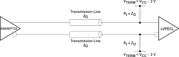
4 Simplified Schematic