SCLS327H March 1996 – October 2014 SN74AHC16244
UNLESS OTHERWISE NOTED, this document contains PRODUCTION DATA.
- 1 Features
- 2 Applications
- 3 Description
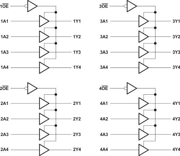
- 4 Simplified Schematic
- 5 Revision History
- 6 Pin Configuration and Functions
-
7 Specifications
- 7.1 Absolute Maximum Ratings
- 7.2 Handling Ratings
- 7.3 Recommended Operating Conditions
- 7.4 Thermal Information
- 7.5 Electrical Characteristics
- 7.6 Switching Characteristics, VCC = 3.3 V ± 0.3 V
- 7.7 Switching Characteristics, VCC = 5 V ± 0.5 V
- 7.8 Noise Characteristics
- 7.9 Operating Characteristics
- 7.10 Typical Characteristics
- 8 Parameter Measurement Information
- 9 Detailed Description
- 10Application and Implementation
- 11Power Supply Recommendations
- 12Layout
- 13Device and Documentation Support
- 14Mechanical, Packaging, and Orderable Information
Package Options
Refer to the PDF data sheet for device specific package drawings
Mechanical Data (Package|Pins)
- DGG|48
- DL|48
- DGV|48
Thermal pad, mechanical data (Package|Pins)
Orderable Information
1 Features
- Members of the Texas Instruments
Widebus™ Family - EPIC™ (Enhanced-Performance Implanted CMOS) Process
- Operating Range 2-V to 5.5-V VCC
- Distributed VCC and GND Pins Minimize
High-Speed Switching Noise - Flow-Through Architecture Optimizes PCB Layout
- Latch-Up Performance Exceeds 250 mA Per JESD 17
- ESD Protection Exceeds 2000 V Per
MIL-STD-883, Method 3015; Exceeds 200 V Using Machine Model (C = 200 pF, R = 0)
2 Applications
3 Description
The SNx4AHC16244 devices are 16-bit buffers and line drivers designed specifically to improve the performance and density of 3-state memory address drivers, clock drivers, and bus-oriented receivers and transmitters.
Device Information(1)
| PART NUMBER | PACKAGE | BODY SIZE (NOM) |
|---|---|---|
| SNx4AHC16244 | SSOP (48) | 15.80 mm × 7.50 mm |
| TSSOP (48) | 12.50 mm 6.10 mm | |
| TVSOP (48) | 9.70 mm 4.40 mm |
- For all available packages, see the orderable addendum at the end of the data sheet.
4 Simplified Schematic