SCAS306K March 1993 – December 2014 SN74LVC827A
PRODUCTION DATA.
- 1 Features
- 2 Applications
- 3 Description/Ordering Information
- 4 Revision History
- 5 Pin Configuration and Functions
- 6 Specifications
- 7 Parameter Measurement Information
- 8 Detailed Description
- 9 Application and Implementation
- 10Power Supply Recommendations
- 11Layout
- 12Device and Documentation Support
- 13Mechanical, Packaging, and Orderable Information
Package Options
Refer to the PDF data sheet for device specific package drawings
Mechanical Data (Package|Pins)
- DGV|24
- DB|24
- DW|24
- PW|24
Thermal pad, mechanical data (Package|Pins)
- DW|24
Orderable Information
1 Features
- Operates From 1.65 V to 3.6 V
- Inputs Accept Voltages to 5.5 V
- Max tpd of 6.7 ns at 3.3 V
- Typical VOLP (Output Ground Bounce)
< 0.8 V at VCC = 3.3 V, TA = 25°C - Typical VOHV (Output VOH Undershoot)
> 2 V at VCC = 3.3 V, TA = 25°C - Supports Mixed-Mode Signal Operation on
All Ports (5-V Input/Output Voltage With
3.3-V VCC) - Ioff Supports Live Insertion, Partial-Power-Down Mode, and Back-Drive Protection
- Latch-Up Performance Exceeds 250 mA Per JESD 17
- ESD Protection Exceeds JESD 22
- 2000-V Human-Body Model
- 200-V Machine Model
- 1000-V Charged-Device Model
2 Applications
- LED Displays
- Network Switches
- Telecom Infrastructure
- Servers
- Motor Drivers
- I/O Expanders
3 Description/Ordering Information
The SN74LVC827A device is a 10-bit buffer/bus driver is designed for 1.65-V to 3.6-V VCC operation.
Device Information(1)
| PART NUMBER | PACKAGE | BODY SIZE (NOM) |
|---|---|---|
| SN74LVC827A | TVSOP (24) | 5.00 mm × 4.40 mm |
| SOIC (24) | 15.40 mm × 7.50 mm | |
| SSOP (24) | 8.20 mm × 5.30 mm |
- For all available packages, see the orderable addendum at the end of the data sheet.
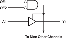
Simplified Schematic