SLOS597B December 2008 – July 2017 TPA6132A2
PRODUCTION DATA.
- 1 Features
- 2 Applications
- 3 Description
- 4 Revision History
- 5 Pin Configuration and Functions
- 6 Specifications
- 7 Detailed Description
- 8 Application and Implementation
- 9 Power Supply Recommendations
- 10Layout
- 11Device and Documentation Support
- 12Mechanical, Packaging, and Orderable Information
Package Options
Refer to the PDF data sheet for device specific package drawings
Mechanical Data (Package|Pins)
- RTE|16
Thermal pad, mechanical data (Package|Pins)
- RTE|16
Orderable Information
1 Features
- Patented DirectPath™ Technology Eliminates Need for DC-Blocking Capacitors
- Outputs Biased at 0 V
- Excellent Low Frequency Fidelity
- Active Click and Pop Suppression
- 2.1 mA Typical Supply Current
- Fully Differential or Single-Ended Inputs
- Built-In Resistors Reduces Component Count
- Improves System Noise Performance
- Constant Maximum Output Power from 2.3 V to 5.5 V Supply
- Simplifies Design to Prevent Acoustic Shock
- Improved RF Noise Immunity
- MicrosoftTM Windows VistaTM Compliant
- High Power Supply Noise Rejection
- 100 dB PSRR at 217 Hz
- 90 dB PSRR at 10 kHz
- Wide Power Supply Range: 2.3 V to 5.5 V
- Gain Settings: –6 dB, 0 dB, 3 dB, and 6 dB
- Short-Circuit and Thermal-Overload Protection
- ±8 kV HBM ESD Protected Outputs
- Small Package Available
- 16-Pin, 3 mm × 3 mm Thin QFN
2 Applications
- Smart Phones / Cellular Phones
- Notebook Computers
- CD / MP3 Players
- Portable Gaming
3 Description
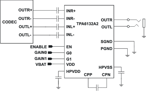
The TPA6132A2 (sometimes referred to as TPA6132) is a DirectPath™ stereo headphone amplifier that eliminates the need for external dc-blocking output capacitors. Differential stereo inputs and built-in resistors set the device gain, further reducing external component count. Gain is selectable at –6 dB, 0 dB, 3 dB or 6 dB. The amplifier drives 25 mW into 16 Ω speakers from a single 2.3 V supply. The TPA6132A2 (TPA6132) provides a constant maximum output power independent of the supply voltage, thus facilitating the design for prevention of acoustic shock.
The TPA6132A2 features fully differential inputs to reduce system noise pickup between the audio source and the headphone amplifier. The high power supply noise rejection performance and differential architecture provides increased RF noise immunity. For single-ended input signals, connect INL+ and INR+ to ground.
The device has built-in pop suppression circuitry to completely eliminate disturbing pop noise during turn-on and turn-off. The amplifier outputs have short-circuit and thermal-overload protection along with ±8 kV HBM ESD protection, simplifying end equipment compliance to the IEC 61000-4-2 ESD standard.
The TPA6132A2 operates from a single 2.3 V to 5.5 V supply with 2.1 mA of typical supply current. Shutdown mode reduces supply current to less than 1 μA.
Device Information(1)
| PART NUMBER | PACKAGE | BODY SIZE (NOM) |
|---|---|---|
| TPA6132A2 | WQFN (16) | 3.00 mm x 3.00 mm |
- For all available packages, see the orderable addendum at the end of the datasheet.
Simplified Schematic
