SLUS909B May 2009 – August 2014 TPS53126
PRODUCTION DATA.
- 1 Features
- 2 Applications
- 3 Description
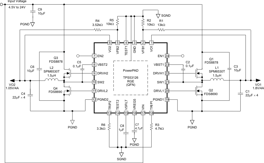
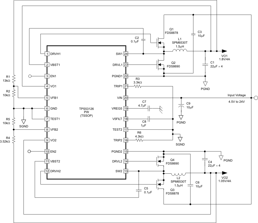
- 4 Simplified Schematics
- 5 Revision History
- 6 Pin Configurations and Functions
- 7 Specifications
-
8 Detailed Description
- 8.1 Overview
- 8.2 Functional Block Diagram
- 8.3
Feature Description
- 8.3.1 PWM Operation
- 8.3.2 Drivers
- 8.3.3 PWM Frequency And Adaptive On-time Control
- 8.3.4 5 Volt Regulator
- 8.3.5 Soft Start
- 8.3.6 Pre-Bias Support
- 8.3.7 Switching Frequency Selection
- 8.3.8 Output Discharge Control
- 8.3.9 Overcurrent Limit
- 8.3.10 Over/under Voltage Protection
- 8.3.11 UVLO Protection
- 8.3.12 Thermal Shutdown
- 8.4 Device Functional Modes
- 9 Application and Implementation
- 10Power Supply Recommendations
- 11Layout
- 12Device and Documentation Support
- 13Mechanical, Packaging, and Orderable Information
Package Options
Refer to the PDF data sheet for device specific package drawings
Mechanical Data (Package|Pins)
- RGE|24
- PW|24
Thermal pad, mechanical data (Package|Pins)
- RGE|24
Orderable Information
1 Features
- D-CAP2™ Mode Control
- Fast Transient Response
- No External Parts Required For Loop Compensation
- Compatible with Ceramic Output Capacitors
- High Initial Reference Accuracy (±1%)
- Low Output Ripple
- Wide Input Voltage Range: 4.5 V to 24 V
- Output Voltage Range: 0.76 V to 5.5 V
- Low-Side RDS(on) Loss-Less Current Sensing
- Adaptive Gate Drivers with Integrated Boost Diode
- Internal 1.2 ms Voltage-Servo Soft Start
- Pre-Biased Soft Start
- Selectable Switching Frequency: 350 kHz / 700 kHz
- Cycle-by-Cycle Over-Current Limiting Control
- 30 mV to 300 mV OCP Threshold Voltage
- Thermally Compensated OCP by 4000 ppm/C° at ITRIP
2 Applications
- Point-of-Load Regulation in Low Power Systems for Wide Range of Applications
- Digital TV Power Supply
- Networking Home Terminal
- Digital Set Top Box (STB)
- DVD Player/Recorder
- Gaming Consoles and Other
3 Description
The TPS53126 is a dual, adaptive on-time, D-CAP2™ mode synchronous Buck controller. The TPS53126 enables system designers to complete the suite of various end equipment's power bus regulators with a cost effective, low external component count, and low standby current solution. The main control loop for the TPS53126 uses the D-CAP2™ mode control which provides a very fast transient response with no external components. The TPS53126 also has a proprietary circuit that enables the device to adapt to both low equivalent series resistance (ESR) output capacitors, such as POSCAP or SP-CAP, and ultra-low ESR ceramic capacitors. The device provides convenient and efficient operation with input voltages from 4.5 V to 24 V and output voltages from 0.76 V to 5.5 V.
The TPS53126 is available in 4mm x 4mm 24 pin VQFN (RGE) or 24 pin TSSOP (PW) packages and is specified from –40°C to 85°C ambient temperature range.
Device Information(1)
| PART NUMBER | PACKAGE | BODY SIZE (NOM) |
|---|---|---|
| TPS53126 | VQFN (24) | 4.00 mm x 4.00 mm |
| TPS53126 | TSSOP (24) | 7.80 mm x 4.40 mm |
- For all available packages, see the orderable addendum at the end of the datasheet.