SLVS576B SEPTEMBER 2005 – January 2016 TPS65150
PRODUCTION DATA.
- 1 Features
- 2 Applications
- 3 Description
- 4 Revision History
- 5 Pin Configuration and Functions
- 6 Specifications
- 7 Detailed Description
-
8 Application and Implementation
- 8.1 Application Information
- 8.2
Typical Application
- 8.2.1 Design Requirements
- 8.2.2
Detailed Design Procedure
- 8.2.2.1 Boost Converter Design Procedure
- 8.2.2.2 Rectifier Diode Selection
- 8.2.2.3 Setting the Output Voltage
- 8.2.2.4 Output Capacitor Selection
- 8.2.2.5 Input Capacitor Selection
- 8.2.2.6 Compensation
- 8.2.2.7 Negative Charge Pump
- 8.2.2.8 Positive Charge Pump
- 8.2.2.9 Gate Voltage Shaping
- 8.2.2.10 Power-On Sequencing
- 8.2.2.11 Fault Delay
- 8.2.2.12 Undervoltage Lockout Function
- 8.2.3 Application Curves
- 8.3 System Examples
- 9 Power Supply Recommendations
- 10Layout
- 11Device and Documentation Support
- 12Mechanical, Packaging, and Orderable Information
Package Options
Refer to the PDF data sheet for device specific package drawings
Mechanical Data (Package|Pins)
- RGE|24
- PWP|24
Thermal pad, mechanical data (Package|Pins)
Orderable Information
1 Features
- 1.8-V to 6-V Input Voltage Range
- Integrated VCOM Buffer
- High-voltage Switch to Isolate V(VGH)
- Gate-Voltage Shaping of V(VGH)
- 2-A Internal MOSFET switch
- Main Output V(VS) up to 15 V With <1% Output Voltage Accuracy
- Virtual-Synchronous Converter Technology
- Regulated Negative Charge Pump Driver V(VGL)
- Regulated Positive Charge Pump Driver V(CPI)
- Adjustable Power-On Sequencing
- Adjustable Fault Detection Timing
- Gate Drive Signal for External Isolation MOSFET
- Out-of-Regulation Protection
- Overvoltage Protection
- Thermal Shutdown
- Available in HTSSOP-24 Package
- Available in VQFN-24 Package
2 Applications
- TFT LCD Displays for Notebooks
- TFT LCD Displays for Monitors
- Car Navigation Displays
3 Description
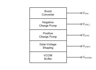
The TPS65150 device offers a very compact and small power supply solution that provides all three voltages required by thin film transistor (TFT) LCD displays. With an input voltage range of 1.8 V to 6 V the device is ideal for notebooks powered by a 2.5-V or 3.3-V input rail or monitor applications with a 5-V input voltage rail. Additionally the TPS65150 device provides an integrated high current buffer to provide the VCOM voltage for the TFT backplane.
Two regulated adjustable charge pump driver provide the positive V(VGH) and negative V(VGL) bias voltages for the TFT. The device incorporates adjustable power-on sequencing for V(VGL) as well as for V(VGH). This avoids any additional external components to implement application specific sequencing. The device has an integrated high-voltage switch to isolate V(VGH).
The same internal circuit can also be used to provide a gate shaping signal of V(VGH) for the LCD panel controlled by the signal applied to the CTRL input. For highest safety, the TPS65150 device has an integrated adjustable shutdown latch feature, which allows application-specific flexibility. The device monitors the outputs (V(VS), V(VGL), V(VGH)); and, as soon as one of the outputs falls below its power good threshold, the device enters shutdown latch, after its adjustable delay time has passed by.
Device Information(1)
| PART NUMBER | PACKAGE | BODY SIZE (NOM) |
|---|---|---|
| TPS65150 | HTSSOP (24) | 7.80 mm × 4.40 mm |
| VQFN (24) | 4.00 mm × 4.00 mm |
- For all available packages, see the orderable addendum at the end of the data sheet.
Block Diagram
