SBVS169D December 2011 – April 2015 TPS7A33
PRODUCTION DATA.
- 1 Features
- 2 Applications
- 3 Description
- 4 Revision History
- 5 Pin Configuration and Functions
- 6 Specifications
- 7 Detailed Description
-
8 Application and Implementation
- 8.1
Application Information
- 8.1.1 Adjustable Operation
- 8.1.2 Capacitor Recommendations
- 8.1.3 Input and Output Capacitor Requirements
- 8.1.4 Noise Reduction and Feed-Forward Capacitor Requirements
- 8.1.5 Post DC-DC Converter Filtering
- 8.1.6 Audio Applications
- 8.1.7 Maximum AC Performance
- 8.1.8 Power-Supply Rejection
- 8.1.9 Output Noise
- 8.1.10 Transient Response
- 8.1.11 Power for Precision Analog
- 8.2 Typical Application
- 8.3 Do's and Don’ts
- 8.1
Application Information
- 9 Power Supply Recommendations
- 10Layout
- 11Device and Documentation Support
- 12Mechanical, Packaging, and Orderable Information
Package Options
Mechanical Data (Package|Pins)
- RGW|20
Thermal pad, mechanical data (Package|Pins)
- RGW|20
Orderable Information
1 Features
- Input Voltage Range: –3 V to –36 V
-
Noise:
- 16 μVRMS (10 Hz to 100 kHz)
-
Power-Supply Ripple Rejection:
- 72 dB (10 kHz)
- Adjustable Output: –1.18 V to –33 V
- Maximum Output Current: 1 A
- Stable With Ceramic Capacitors ≥ 10 μF
- Built-In Current-Limit and Thermal Shutdown Protection
- Available in an External Heatsink-Capable, High Thermal Performance TO-220 Package
- Operating Temperature Range:
–40°C to 125°C
2 Applications
- Supply Rails for Operational Amplifiers, DACs, ADCs, and Other High-Precision Analog Circuitry
- Audio
- Post DC-DC Converter Regulation and Ripple Filtering
- Test and Measurement
- Medical
- Industrial Instrumentation
- Base Stations and Telecom Infrastructure
- 12-V and 24-V Industrial Buses
3 Description
The TPS7A33 series of linear regulators are negative voltage (–36 V), ultralow-noise (16-μVRMS, 72-dB PSRR) linear regulators capable of sourcing a maximum load of 1 A.
The TPS7A33 series include a complementary metal oxide semiconductor (CMOS) logic-level-compatible enable pin (EN) to allow for user-customizable power management schemes. Other features available include built-in current limit and thermal shutdown features to protect the device and system during fault conditions.
The TPS7A33 family is designed using bipolar technology primarily for high-accuracy, high-precision instrumentation applications, where clean voltage rails are critical to maximize system performance. This feature makes it ideal to power operational amplifiers, analog-to-digital converters (ADCs), digital-to-analog converters (DACs), and other high-performance analog circuitry.
In addition, the TPS7A33 family of linear regulators is suitable for post DC-DC converter regulation. By filtering out the output voltage ripple inherent to DC-DC switching conversion, maximum system performance is ensured in sensitive instrumentation, medical, test and measurement, audio, and RF applications.
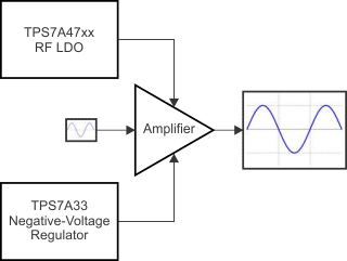
For applications where positive and negative high-performance rails are required, consider the TPS7A4700 positive high-voltage, ultralow-noise, low-dropout linear regulator as well.
Device Information(1)
| PART NUMBER | PACKAGE | BODY SIZE (NOM) |
|---|---|---|
| TPS7A33 | TO-220 (7) | 10.17 mm × 8.38 mm |
| VQFN (20) | 5.00 mm × 5.00 mm |
- For all available packages, see the orderable addendum at the end of the data sheet.
