SLVSD64 December 2015 TPS7A6650H-Q1
PRODUCTION DATA.
- 1 Features
- 2 Applications
- 3 Description
- 4 Revision History
- 5 Pin Configuration and Functions
- 6 Specifications
- 7 Detailed Description
- 8 Application and Implementation
- 9 Power Supply Recommendations
- 10Layout
- 11Device and Documentation Support
- 12Mechanical, Packaging, and Orderable Information
Package Options
Mechanical Data (Package|Pins)
- DGN|8
Thermal pad, mechanical data (Package|Pins)
- DGN|8
Orderable Information
1 Features
- Qualified for Automotive Applications
- AEC-Q100 Qualified With the Following Results:
- Device Temperature: –40°C to 150°C Ambient Operating Temperature Range
- Device HBM ESD Classification Level H2
- Device CDM ESD Classification Level C4
- 4-V to 40-V Wide Vin Input Voltage Range With up to 45-V Transient
- Output Current: 50 mA
- Low Quiescent Current, I(q):
- 2 µA when EN = Low (Shutdown Mode)
- 12 µA Typical at Light Loads
- Low ESR Ceramic Output Stability Capacitor (2.2 µF–100 µF)
- 130-mV Dropout Voltage at 50 mA
(Typical, V(Vin) = 4 V) - Fixed 5-V Output Voltage
- Low Input Voltage Tracking
- Integrated Power-On Reset
- Programmable Reset-Pulse Delay
- Open-Drain Reset Output
- Integrated Fault Protection
- Thermal Shutdown
- Short-Circuit Protection
- 8-Pin MSOP-DGN Package
2 Applications
- Powertrain Sensor Module
- Infotainment Systems With Sleep Mode
- Body Control Modules
- Always-On Battery Applications
- Gateway Applications
- Remote Keyless Entry Systems
- Immobilizers
3 Description
The TPS7A6650H-Q1 is a low-dropout linear regulator designed for up to 40-V Vin operations. With only 12-µA quiescent current at no load, it is quite suitable for standby microprocessor control-unit systems, especially in automotive applications.
The device features integrated short-circuit and overcurrent protection. The device implements reset delay on power up to indicate the output voltage is stable and in regulation. One can program the delay with an external capacitor. A low-voltage tracking feature allows for a smaller input capacitor and can possibly eliminate the need of using a boost converter during cold-crank conditions.
The device operates in the –40°C to 150°C temperature range, which makes it well suited for power supplies in various automotive applications.
Device Information(1)
| DEVICE NUMBER | PACKAGE | BODY SIZE (NOM) |
|---|---|---|
| TPS7A6650H-Q1 | HVSSOP (8) | 3.00 mm × 3.00 mm |
- For all available packages, see the orderable addendum at the end of the datasheet.
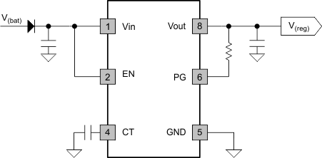
Hardware-Enable Option
