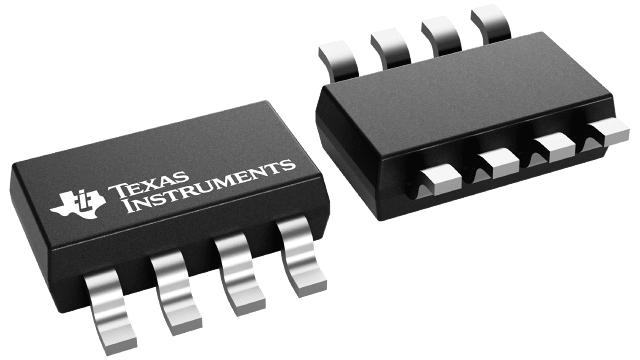
Packaging information
| Package | Pins SOT-23-THN (DDF) | 8 |
| Operating temperature range (°C) -40 to 125 |
| Package qty | Carrier 3,000 | LARGE T&R |
Features for the INA630
- Optimized for cost and size sensitive applications
- Super-beta bipolar precision:
- High common-mode rejection: 126dB (minimum) for G = 20V/V to 1000V/V
- Low offset voltage: 60µV (typical), 350µV (maximum)
- Low offset voltage drift: 0.7µV/°C (typical), 2µV/°C (maximum)
- Low gain non-linearity: 10ppm (G = 100V/V) (maximum)
- High power supply rejection: 123dB (minimum) for G = 20V/V to 1000V/V
- Voltage noise density: 40nV/√Hz at f = 1kHz
- Gain set with external resistor divider for G ≥
20V/V
- Maximum differential input voltages of ±125mV
- Bandwidth: 550kHz (G = 20), 100kHz (G = 100)
- Supply range:
- Single-supply: 4.5V to 36V
- Dual-supply: ±2.25V to ±18V
- Supply current: 300µA (typical)
- Specified temperature range: –40°C to +125°C
Description for the INA630
The INA630 is a high-precision instrumentation amplifier that offers low power consumption and operates over a wide single-supply or dual-supply range. The INA630 is optimized for small differential voltages (±125mV maximum) while providing excellent common-mode suppression (126dB CMRR). The INA630 offers flexible gain setting with an external resistor divider of minimum G = 20V/V.
The INA630 is based on an indirect current feedback architecture that offers low gain error and non-linearity. Due to the architecture the reference pin impedance does not degrade the CMRR performance. The device enables wider input and output voltage range compared to traditional instrumentation amplifiers. The device has high precision as a result of super-beta input transistors, which provide low input offset voltage, offset voltage drift, low bias current and current noise.