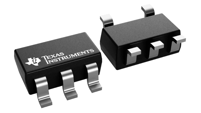
Packaging information
| Package | Pins SOT-23 (DBV) | 5 |
| Operating temperature range (°C) -40 to 125 |
| Package qty | Carrier 3,000 | LARGE T&R |
Features for the SN74LVC1G86
- Qualified from –40°C to +125°C
- Supports 5V VCC operation
- Inputs are over voltage tolerant up to 5.5V
- Supports down translation to VCC
- Maximum tpd of 4ns at 3.3V and 15pF load
- Low power consumption, 10µA maximum ICC at 85°C
- ±24mA output drive at 3.3V
- Ioff supports partial-power-down mode, and back-drive protection
- Available in the Texas Instruments NanoFree™ package
- Latch-up performance exceeds 100mA per JESD 78, Class II
Description for the SN74LVC1G86
The SN74LVC1G86 device performs the Boolean function Y = AB + A B in positive logic. This single 2-input exclusive-OR gate is designed for operation from 1.65V to 5.5V VCC.
If the input is low, the other input is reproduced in true form at the output. If the input is high, the signal on the other input is reproduced inverted at the output. This device has low power consumption with maximum tpd of 4ns at 3.3V and 15pF capacitive load. The maximum output drive is ±32mA at 4.5V and ±24mA at 3.3V.
This device is fully specified for partial-power-down applications using Ioff. The Ioff circuitry disables the outputs, preventing damaging current back flow through the device when it is powered down.